Intel Xeon "Sapphire Rapids" Memory Detailed, Resembles AMD 1st Gen EPYC: Decentralized 8-Channel DDR5
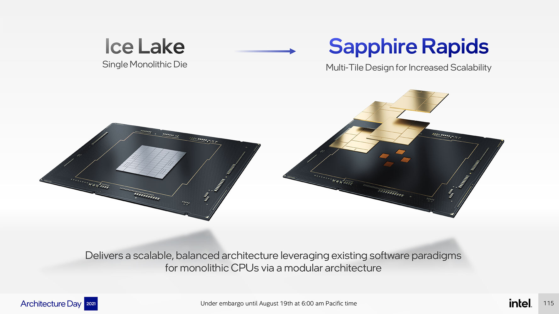
Intel's upcoming Xeon "Sapphire Rapids" processor features a memory interface topology that closely resembles that of first-generation AMD EPYC "Rome," thanks to the multi-chip module design of the processor. Back in 2017, Intel's competing "Skylake-SP" Xeon processors were based on monolithic dies. Despite being spread across multiple memory controller tiles, the 6-channel DDR4 memory interface was depicted by Intel as an advantage over EPYC "Rome." AMD's first "Zen" based enterprise processor was a multi-chip module of four 14 nm, 8-core "Zeppelin" dies, each with a 2-channel DDR4 memory interface that added up to the processor's 8-channel I/O. Much like "Sapphire Rapids," a CPU core from any of the four dies had access to memory and I/O controlled by any other die, as the four were networked over the Infinity Fabric interconnect in a configuration that essentially resembled "4P on a stick."
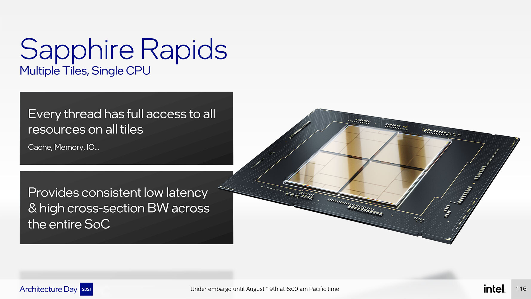
With "Sapphire Rapids," Intel is taking a largely similar approach—it has four compute tiles (dies) instead of a monolithic die, which Intel says helps with scalability in both directions; and each of the four compute tiles has a 2-channel DDR5 or 1024-bit HBM memory interface, which add up to the processor's 8-channel DDR5 total I/O. Intel says that CPU cores from each tile has equal access to memory, last-level cache, and I/O controlled by another die. Inter-tile communication is handled by EMIB physical media (55 micron bump-pitch wiring). UPI 2.0 makes up the inter-socket interconnect. Each of the four compute tiles has 24 UPI 2.0 links that operate at 16 GT/s. Intel didn't detail how memory is presented to the operating system, or the NUMA hierarchy, however much of Intel's engineering effort appears to be focused on making this disjointed memory I/O work as if "Sapphire Rapids" were a monolithic die. The company claims "consistent low-latency, high cross-sectional bandwidth across the SoC."


With "Sapphire Rapids," Intel is taking a largely similar approach—it has four compute tiles (dies) instead of a monolithic die, which Intel says helps with scalability in both directions; and each of the four compute tiles has a 2-channel DDR5 or 1024-bit HBM memory interface, which add up to the processor's 8-channel DDR5 total I/O. Intel says that CPU cores from each tile has equal access to memory, last-level cache, and I/O controlled by another die. Inter-tile communication is handled by EMIB physical media (55 micron bump-pitch wiring). UPI 2.0 makes up the inter-socket interconnect. Each of the four compute tiles has 24 UPI 2.0 links that operate at 16 GT/s. Intel didn't detail how memory is presented to the operating system, or the NUMA hierarchy, however much of Intel's engineering effort appears to be focused on making this disjointed memory I/O work as if "Sapphire Rapids" were a monolithic die. The company claims "consistent low-latency, high cross-sectional bandwidth across the SoC."