Wednesday, July 25th 2018

Intel Core i9 8-core LGA1151 Processor Could Get Soldered IHS, Launch Date Revealed

The fluid thermal interface material between the processor die and the IHS (integrated heatspreader) has been a particularly big complaint of PC enthusiasts in recent times, especially given that AMD has soldered IHS (believed to be more effective in heat-transfer), across its Ryzen processor line. We're getting reports of Intel planning to give at least its top-dog Core i9 "Whiskey Lake" 8-core socket LGA1151 processor a soldered IHS. The top three parts of this family have been detailed in our older article.

The first Core i9 "Whiskey Lake" SKU is the i9-9900K, an 8-core/16-thread chip clocked between 3.60~5.00 GHz, armed with 16 MB of L3 cache. The introduction of the Core i9 extension to the mainstream desktop segment could mean Intel is carving out a new price point for this platform that could be above the $300-350 price traditionally held by top Core i7 "K" SKUs from the previous generations. In related news, we are also hearing that the i9-9900K could be launched as early as 1st August, 2018. This explains why motherboard manufacturers are in such hurry to release BIOS updates for their current 300-series chipset motherboards.
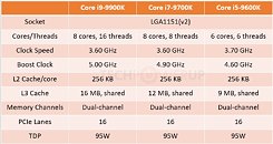
Source: Coolaler
Add your own comment

79 Comments on Intel Core i9 8-core LGA1151 Processor Could Get Soldered IHS, Launch Date Revealed

#26
Prima.Vera
Guessing next year will finally be the year to get an upgrade after 7 (seven) years (i9 -9700K + 1180Ti + DDR4 + NVMe drive)
Posted on Reply
#27
newtekie1
Semi-Retired Folder
R0H1Tworst of all you couldn't solder them all because the chip was tiny!
This was kind of the only legit reasoning. There was a really good article about the challenges of soldering a small die. The issue is when the solder cools and slightly contracts, it actually pulls on the IHS and die. You have to have really good adhesion to both, or the solder can actually separate from the die or IHS. The more surface area you have to attach to, obviously the better adhesion you can get. So smaller dies are harder to solder.

But now with the 8-core dies of the 9900k, it likely is a big enough die to make soldering easy enough for Intel to do it. And the switch from solder to TIM was also a fault of Intel's stagnation, sticking with the same 4-core die for so long, and just doing process shrinks, lead to very small physical cores. If they had move the mainstream up sooner, like they should have, then the dies would have been large enough to make solder a viable option.
R0H1TAMD doesn't solder RR, they solder everything else AFAIK, unlike Intel.
So not the entire series then.
Posted on Reply
#28
Valantar
newtekie1Except AMD doesn't. But who cares about pesky details like that, right?
They do, actually. Not the APUs, but those are based off a different die. As such, they're not from the same wafers - and thus don't apply to what I was describing.
Posted on Reply
#29
phill
newtekie1Do you really have a need for more than the 40 PCI-E 3.0 lanes that the 1151 platform provides?

Except AMD doesn't. But who cares about pesky details like that, right?
I suppose it would depend if you have SLI, M.2 drives and the like.. I'm not sure I understand the logic behind limiting the lanes if CPUs that cost the same money or less have them all unlocked but I suppose that's how they get you to buy the higher spec models..
I think the 5820k had 28 lanes, so did the 5930k? Was it the 5960X that only had the full 40 lanes? Same went for the 6xxx series and such I believe. I don't think it was until the 5xxx series CPUs that the limitation was brought in was it?
Posted on Reply
#30
R0H1T
newtekie1This was kind of the only legit reasoning. There was a really good article about the challenges of soldering a small die. The issue is when the solder cools and slightly contracts, it actually pulls on the IHS and die. You have to have really good adhesion to both, or the solder can actually separate from the die or IHS. The more surface area you have to attach to, obviously the better adhesion you can get. So smaller dies are harder to solder.

But now with the 8-core dies of the 9900k, it likely is a big enough die to make soldering easy enough for Intel to do it. And the switch from solder to TIM was also a fault of Intel's stagnation, sticking with the same 4-core die for so long, and just doing process shrinks, lead to very small physical cores. If they had move the mainstream up sooner, like they should have, then the dies would have been large enough to make solder a viable option.


So not the entire series then.
This was a possible reason but never proved to be the official company line. As for the challenges, we have 14nm Ryzen delidded, with IHS, while 22nm Haswell is not. Needless to say that Haswell is not much smaller than Ryzen, if at all. Besides that theory gets torn to shreds when talking about Intel HEDT.


As for RR, I can see ASP being the reason why AMD did this. I won't defend it but I can see why it's unsustainable, given the volumes & margin on that part.
Posted on Reply
#31
VulkanBros
FreedomEclipsereasons?
It´s cheaper, the IHS is soldered and more often than Intel, they make new CPU´s compatible with older boards (or older boards compatible for new CPU´s - via BIOS updates) - and AMD boards tend to be cheaper - and because I like the new RyZen/ThreadRipper generation CPU´s in general.
Posted on Reply
#32
newtekie1
Semi-Retired Folder
ValantarThey do, actually. Not the APUs, but those are based off a different die. As such, they're not from the same wafers - and thus don't apply to what I was describing.
But they are part of the same series of CPUs. So, hence, the entire series is not soldered.
phillI suppose it would depend if you have SLI, M.2 drives and the like.. I'm not sure I understand the logic behind limiting the lanes if CPUs that cost the same money or less have them all unlocked but I suppose that's how they get you to buy the higher spec models..
I think the 5820k had 28 lanes, so did the 5930k? Was it the 5960X that only had the full 40 lanes? Same went for the 6xxx series and such I believe. I don't think it was until the 5xxx series CPUs that the limitation was brought in was it?
Yes, but even with SLI and multiple M.2 drives, the 40 lanes that an 8700K on a Z370 motherboard provides is more than enough. Even if you've got two GPUs, and two high speed M.2 drives, that's only 24 lanes total, leaving another 16 for other devices. There is that much more you can put on a board that needs 16 lanes of PCI-E bandwidth.
R0H1TThis was a possible reason but never proved to be the official company line. As for the challenges, we have 14nm Ryzen delidded, with IHS, while 22nm Haswell is not. Needless to say that Haswell is not much smaller than Ryzen, if at all. Besides that theory gets torn to shreds when talking about Intel HEDT.
You can post all the off angle pictures you want, the reality is Summit Ridge die is actually significantly bigger than Ivy Bridge and Haswell. Summit Ridge is 192mm2, Ivy Bridge was only 160mm2. To give an idea, Sandy Bridge was 216mm2. So that is a pretty big jump down, and certainly a plausible reason why they decided to switch to TIM with Ivy Bridge. Moving forward after that, they just stuck with the decision, even as the dies started getting bigger again. And eventually did make the stupid move to just do TIM on everything, probably because they realized it was easier.
Posted on Reply
#34
FreedomEclipse
~Technological Technocrat~
VulkanBrosIt´s cheaper, the IHS is soldered and more often than Intel, they make new CPU´s compatible with older boards (or older boards compatible for new CPU´s - via BIOS updates) - and AMD boards tend to be cheaper - and because I like the new RyZen/ThreadRipper generation CPU´s in general.
but Intel totally smashes it in gaming still due to faster single core speed.
Posted on Reply
#35
Tsukiyomi91
still have a whole lot higher clock speeds with all cores under full load.
Posted on Reply
#36
ShurikN
newtekie1But they are part of the same series of CPUs. So, hence, the entire series is not soldered.
It depends on what you consider a "series". uArch or naming number...
To me saying Raven Ridge and Summit Ridge are the same series of cpus is like saying the same for 7700K and 7900X. They both start with a 7, but they couldn't be any more different...
Posted on Reply
#37
R0H1T
newtekie1You can post all the off angle pictures you want, the reality is Summit Ridge die is actually significantly bigger than Ivy Bridge and Haswell. Summit Ridge is 192mm2, Ivy Bridge was only 160mm2. To give an idea, Sandy Bridge was 216mm2. So that is a pretty big jump down, and certainly a plausible reason why they decided to switch to TIM with Ivy Bridge. Moving forward after that, they just stuck with the decision, even as the dies started getting bigger again. And eventually did make the stupid move to just do TIM on everything, probably because they realized it was easier.
I said Haswell, GT2 (i7) is 177mm^2 while GT3(Iris) is 264 mm^2 so not much smaller than SR. What about the discrepancy with Intel HEDT, since they're much bigger dies?

Cheaper IMO, why would it be easier given they still make soldered CPU's & seemingly are going back to solder for the upcoming i9.
Posted on Reply
#38
Valantar
newtekie1But they are part of the same series of CPUs. So, hence, the entire series is not soldered.
No, they're not. Sure, they share a model number series. But so does Threadripper. As does Intel HEDT with Intel MSDT, for that matter. Are those also the same series? No. RR is a separate series from standard Ryzen, as shown by the entirely different die used. Intel doesn't have a comparable series (due to having iGPUs across all MSDT chips), but that doesn't change the fact that RR is not the same as other Ryzen.
newtekie1Yes, but even with SLI and multiple M.2 drives, the 40 lanes that an 8700K on a Z370 motherboard provides is more than enough. Even if you've got two GPUs, and two high speed M.2 drives, that's only 24 lanes total, leaving another 16 for other devices. There is that much more you can put on a board that needs 16 lanes of PCI-E bandwidth.
For demanding uses, you really can't say that Z/H370-based systems have "40 lanes". That's only true as long as no more than 4 of the 24 from the PCH are used at one time. Sure, this is an edge case not relevant to the vast majority of users, but doubling the QPI speed would make this bottleneck go away for even heavy users with 10GbE NICs and multiple SSDs. Also, the lack of support for lane bifurcation makes those lanes (including the CPU ones) far less flexible than they ought to be.
Posted on Reply
#39
Assimilator
newtekie1Yes, but even with SLI and multiple M.2 drives, the 40 lanes that an 8700K on a Z370 motherboard provides is more than enough. Even if you've got two GPUs, and two high speed M.2 drives, that's only 24 lanes total, leaving another 16 for other devices.
Another one drinking the "40 lanes" Kool-Aid. On Z270 there are 16 lanes directly from the CPU and 24 lanes from the chipset, and the chipset talks to the CPU over a 4-lane link. That means that if you have two 4-lane M.2 SSDs hanging off the chipset, and you try to access them both at the same time (example: RAID), they are going to be bottlenecked. Furthermore, of the 24 chipset lanes at least half will already be taken by other peripherals (SATA, USB, LAN) so you will get maybe 12 lanes max off there... maybe. That's not taking into account that you get, at maximum, 16 lanes from the CPU for graphics cards - regardless of whether you have one or two GPUs.

Now, whether an effective 28 PCIe 3.0 lanes is too little for the average midrange gamer with 1 GPU and 1 M.2 drive is another story altogether.
Posted on Reply
#40
CrAsHnBuRnXp
VulkanBrosWhy not just buy an AMD CPU.......
Like it's going to outperform Intel...

AMD has gotten way better. But not that much better.
Posted on Reply
#41
newtekie1
Semi-Retired Folder
ShurikNIt depends on what you consider a "series". uArch or naming number...
To me saying Raven Ridge and Summit Ridge are the same series of cpus is like saying the same for 7700K and 7900X. They both start with a 7, but they couldn't be any more different...
ValantarNo, they're not. Sure, they share a model number series. But so does Threadripper. As does Intel HEDT with Intel MSDT, for that matter. Are those also the same series? No. RR is a separate series from standard Ryzen, as shown by the entirely different die used. Intel doesn't have a comparable series (due to having iGPUs across all MSDT chips), but that doesn't change the fact that RR is not the same as other Ryzen.
Same socket, in the same product stack = same series. It doesn't matter that they use a different die, the 2 core Intels and 4 core and 6 cores use different dies too, they are still the same series of CPUs. You are not going to be able to successfully argue that the Ryzen 5 2400G and Ryzen 5 2600 are two different series of processors. They might have different cores in them, but AMD has made them the same series. What was said would have been true back when the APUs were separate from the mainstream deaktop processor, on a complete different platform with a completely different naming scheme, but that is no longer the case. AMD has made them the same series as their traditional CPU line.
ValantarFor demanding uses, you really can't say that Z/H370-based systems have "40 lanes". That's only true as long as no more than 4 of the 24 from the PCH are used at one time. Sure, this is an edge case not relevant to the vast majority of users, but doubling the QPI speed would make this bottleneck go away for even heavy users with 10GbE NICs and multiple SSDs. Also, the lack of support for lane bifurcation makes those lanes (including the CPU ones) far less flexible than they ought to be.
AssimilatorAnother one drinking the "40 lanes" Kool-Aid. On Z270 there are 16 lanes directly from the CPU and 24 lanes from the chipset, and the chipset talks to the CPU over a 4-lane link. That means that if you have two 4-lane M.2 SSDs hanging off the chipset, and you try to access them both at the same time (example: RAID), they are going to be bottlenecked.
That isn't how it works with DMA, the data does not have to flow back to the CPU to be moved around. Every bit of data transferred over the PCI-E bus isn't going through the CPU. The data flows through the chipset, so the 4 lane connection back to the CPU is almost never a bottleneck. The only time it is really a bottleneck is for the GPUs, which is why they are wired directly to the CPU and everything else happily flows through the chipset. Have you ever looked at how the HEDT boards are wired? Those extra CPU PCI-E lanes aren't used for storage... The only other time the 4x link between the chipset and CPU is stressed is loading data from a RAID0 M.2 NVMe setup into memory(program loading, game level loading, etc.) But you still get almost 4GB/s of transfer speed from the drives into Memory. Are you really going to notice a faster transfer speed than that? Besides that, in situations where you are loading data from the drives into memory, those are almost always random read/write cases. And even the best drives on the market right now don't even break 1GB/s random read, so even if you had two in RAID0, you're not coming close to a bottleneck on the DMI link between the chipset and the CPU.
AssimilatorFurthermore, of the 24 chipset lanes at least half will already be taken by other peripherals (SATA, USB, LAN) so you will get maybe 12 lanes max off there... maybe.
Bull. SATA, USB, and LAN are all provided by the chipset without using any of the 24 PCI-E lanes. All the extra peripherals likely would never need 12 PCI-E 3.0 lanes, even on a high end board. You've got a sound card taking up 1 lane, maybe another LAN port taking up another, perhaps a wifi card taking up 1 more, and them maybe they add a USB3.1 controller taking 1 or maybe 2 more. Perhaps they even want to use an extra SATA controller taking 1 more. So the extras taking maybe 5 lanes, call it 6 to be safe? Certainly not half of the 24 provided.
R0H1TI said Haswell, GT2 (i7) is 177mm^2 while GT3(Iris) is 264 mm^2 so not much smaller than SR. What about the discrepancy with Intel HEDT, since they're much bigger dies?

Cheaper IMO, why would it be easier given they still make soldered CPU's & seemingly are going back to solder for the upcoming i9.
My point is that Ivy Bridge was the issue. My opinion of what happened is that when they were getting Ivy Bridge ready they ran into problems with the solder, and decided to just switch to TIM instead of trying to find an engineering solution to allow them to use solder. Then they just never bothered to switch back, either because they were too lazy or they just noticed the difference in the bottom line and liked the slightly heavier wallets. The fact that they switch the HEDT over to TIM too kind of points to them liking their heavy wallets. But my point was, originally, it was because of the very much smaller die of Ivy Bridge and the challenges it presented.
Posted on Reply
#42
R0H1T
newtekie1My point is that Ivy Bridge was the issue. My opinion of what happened is that when they were getting Ivy Bridge ready they ran into problems with the solder, and decided to just switch to TIM instead of trying to find an engineering solution to allow them to use solder. Then they just never bothered to switch back, either because they were too lazy or they just noticed the difference in the bottom line and liked the slightly heavier wallets. The fact that they switch the HEDT over to TIM too kind of points to them liking their heavy wallets. But my point was, originally, it was because of the very much smaller die of Ivy Bridge and the challenges it presented.
That's exactly what I'm contesting, this was a popular theory but never proven. With the i9 the die size could be 10~20% bigger than 8700k, if Intel uses solder then there's absolutely no reason why they shouldn't have gone for solder on the unlocked hexa core ~ except saving money! Which frankly put, shows them in a very bad light.
Posted on Reply
#43
hat
Enthusiast
newtekie1You can post all the off angle pictures you want, the reality is Summit Ridge die is actually significantly bigger than Ivy Bridge and Haswell. Summit Ridge is 192mm2, Ivy Bridge was only 160mm2. To give an idea, Sandy Bridge was 216mm2. So that is a pretty big jump down, and certainly a plausible reason why they decided to switch to TIM with Ivy Bridge.
Smaller dies have been soldered in the past. According to our own database, the C2D E6600 was even smaller than Ivy Bridge, and it was soldered.
Posted on Reply
#44
Axaion
>(believed to be more effective in heat-transfer)


Come on now, we all know you know better, its pretty obvious solder has way better heat transfer than toothpaste
Posted on Reply
#45
newtekie1
Semi-Retired Folder
hatSmaller dies have been soldered in the past. According to our own database, the C2D E6600 was even smaller than Ivy Bridge, and it was soldered.
Interesting. I guess there goes my theory, Intel's just cheap.
Posted on Reply
#46
MxPhenom 216
ASIC Engineer
Who fucking cares about solder. The solder vs TIM debate is a dead horse that people are obsessed with beating every time a new chip comes out. Not to mention people lacking technical understanding for why chips weren't being soldered. And its not really a money grab.
newtekie1Interesting. I guess there goes my theory, Intel's just cheap.
I dont think its just die size that matters. But PCB thickness too. Pcbs for intel chips got pretty thin when Haswell came. Im not sure if they stayed that way but i wouldnt be surprised.
Posted on Reply
#47
hat
Enthusiast
What reason is there for them not to be soldered? It's far better than paste. Better thermal transfer results in lower temps. That isn't a bad thing... especially when for the average user, many of these chips are being held back by high temps. Combine that with the rest of the cash grabby things Intel has been doing these past several years and you've got yourself one heck of a crap shoot.
Posted on Reply
#48
MxPhenom 216
ASIC Engineer
newtekie1Interesting. I guess there goes my theory, Intel's just cheap.
I dont think its just die size that matters. But PCB thickness too. Pcbs for intel chips got pretty thin when Haswell came. Im not sure if they stayed that way but i wouldnt be surprised.
hatWhat reason is there for them not to be soldered? It's far better than paste. Better thermal transfer results in lower temps. That isn't a bad thing... especially when for the average user, many of these chips are being held back by high temps. Combine that with the rest of the cash grabby things Intel has been doing these past several years and you've got yourself one heck of a crap shoot.
Well lets face it. Overclocking is pretty dead with the clock speeds these chips are pushing from Turbo Boost out of the box. Because of this i dont really give a shit whats between the IHS and die.
Posted on Reply
#50
Valantar
newtekie1Same socket, in the same product stack = same series. It doesn't matter that they use a different die, the 2 core Intels and 4 core and 6 cores use different dies too, they are still the same series of CPUs. You are not going to be able to successfully argue that the Ryzen 5 2400G and Ryzen 5 2600 are two different series of processors. They might have different cores in them, but AMD has made them the same series. What was said would have been true back when the APUs were separate from the mainstream deaktop processor, on a complete different platform with a completely different naming scheme, but that is no longer the case. AMD has made them the same series as their traditional CPU line.
1)Intel doesn't have 2-core desktop dice, only 4- and 6. The rest are harvested/disabled.
2) The difference between Raven Ridge and Summit/Pinnacle Ridge is far bigger than between any mainstream Intel chips, regardless of differences in core count. The Intel 4+2 and 6+2 dice are largely identical except for the 2 extra cores. All Summit/Pinnacle Ridge chips (and Threadripper) are based off the same 2-CCX iGPU-less die (well, updated/tuned for Pinnacle Ridge and the updated process node, obviously). Raven Ridge is based off an entirely separate die design with a single CCX, an iGPU, and a whole host of other uncore components belonging to that. The difference is comparable to if not bigger than the difference between the ring-bus MSDT and the mesh-interconnect HEDT Intel chips.
3) If "Same socket, in the same product stack" is the rule, do you count Kaby Lake-X as the same series as Skylake-X?
4) "Same product stack" is also grossly misleading. From the way you present this, Intel has one CPU product stack - outside of the weirdly named low-end core-based Pentium and Celerons, that is, which seem to "lag" a generation or two in their numbering. They all use the same numbering scheme, from mobile i3s to HEDT 18-core i9s. But you would agree that the U, H and other suffixes for mobile chips place them in a different product stack, no? Or would you say that Intel has no mobile product stack? 'Cause if you think they do, then you have to agree that the G suffix of the desktop RR APUs also makes that a separate product stack. Not to mention naming: Summit and Pinnacle Ridge are "Ryzen". Then there's "Ryzen Threadripper". Then there's "Ryzen with Vega Graphics". Subsets? Sure. Both are. But still separate stacks.
newtekie1That isn't how it works with DMA, the data does not have to flow back to the CPU to be moved around. Every bit of data transferred over the PCI-E bus isn't going through the CPU. The data flows through the chipset, so the 4 lane connection back to the CPU is almost never a bottleneck. The only time it is really a bottleneck is for the GPUs, which is why they are wired directly to the CPU and everything else happily flows through the chipset. Have you ever looked at how the HEDT boards are wired? Those extra CPU PCI-E lanes aren't used for storage... The only other time the 4x link between the chipset and CPU is stressed is loading data from a RAID0 M.2 NVMe setup into memory(program loading, game level loading, etc.) But you still get almost 4GB/s of transfer speed from the drives into Memory. Are you really going to notice a faster transfer speed than that? Besides that, in situations where you are loading data from the drives into memory, those are almost always random read/write cases. And even the best drives on the market right now don't even break 1GB/s random read, so even if you had two in RAID0, you're not coming close to a bottleneck on the DMI link between the chipset and the CPU.
You're right that DMA alleviates this somewhat, but that depends on the workload. Is all you do with your SSDs copying stuff between them? If not, the data is going to go to RAM or CPU. If you have a fast NIC, have you made sure that the drive you're downloading to/uploading from is connected off the PCH and not the CPU? 'Cause if not, you're - again - using that QPI link. And so on, and so on. The more varied your load, the more that link is being saturated. And again, removing the bottleneck almost entirely would not be difficult at all - Intel would just have to double the lanes for the uplink. This would require a tiny increase in die space on the CPUs and PCHes, and somewhat more complex wiring in the motherboard, but I'm willing to bet the increase in system cost would be negligible.
newtekie1Bull. SATA, USB, and LAN are all provided by the chipset without using any of the 24 PCI-E lanes. All the extra peripherals likely would never need 12 PCI-E 3.0 lanes, even on a high end board. You've got a sound card taking up 1 lane, maybe another LAN port taking up another, perhaps a wifi card taking up 1 more, and them maybe they add a USB3.1 controller taking 1 or maybe 2 more. Perhaps they even want to use an extra SATA controller taking 1 more. So the extras taking maybe 5 lanes, call it 6 to be safe? Certainly not half of the 24 provided.
Apparently you're not familiar with Intel HSIO/Flex-IO or the feature sets of their chipsets. You're partially right that USB is provided - 2.0 and 3.0, but not 3.1 except for the 300-series excepting the Z370 (which is really just a rebranded Z270). Ethernet is done through separate controllers over PCIe, and SATA shares lanes with PCIe. Check out the HSIO lane allocation chart from AnandTech's Z170 walkthrough from the Skylake launch - the only major difference between this and Z270/370 is the addition of a sixth PCIe 3.0x4 controller, for 4 more HSIO lanes. How they can be arranged/split (and crucially, how they can not) works exactly the same. Note that Intel's PCH spec sheets (first picture here) always say "up to" X number of USB ports/PCIe lanes and so on - due to them being interchangeable. Want more than 6 USB 3.0 ports? That takes away an equivalent amount of PCIe lanes. Want SATA ports? All of those occupy RST PCIe lanes, though at least some can be grouped on the same controller. Want dual Ethernet? Those will eat PCIe lanes too. And so on. The moral of the story: An implemented Intel chipset does not have the amount of available PCIe lanes that they advertise that it has.
OctopussHow about overclocking.guide/the-truth-about-cpu-soldering/ ?
That jives pretty well with der8auers recent look into the question of "can you solder an IHS yourself?", but with one major caveat: the difference in complexity and cost between doing a one-off like the process shown there and doing the same on an industrial scale should really not be underestimated. Intel already knows how to to this. They already own the tools and machinery, as they've done this for years. Intel can buy materials at bargain-basement bulk costs. Intel has the engineering expertise to minimize the occurrence of cracks and faults. And it's entirely obvious that an industrial-scale process like this would be fine-tuned to minimize the soldering process causing cracked dice and other failures.
Posted on Reply
Add your own comment
Jul 16th, 2024 07:47 EDT change timezone

New Forum Posts

Popular Reviews

Controversial News Posts