Monday, November 5th 2018

SK Hynix Launches World's First 'CTF-based 4D NAND Flash' (96-Layer 512Gb TLC)
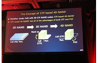
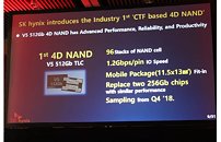
SK Hynix today launched the world's first 96-Layer 512Gb CTF (Charge Trap Flash) based 4D NAND flash. Don't let the name trick you - it's still based on 3D TLC technology, but SK Hynix has gone and added a 4th dimension due to its pairing of charge trap flash technology in conjunction with PUC (Peri. Under Cell technology.
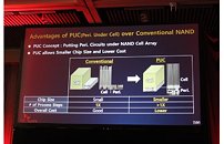
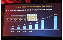
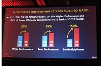
SK Hynix says that their approach is (obviously) better than the industry-wide 3D Floating Gate approach. The 4D NAND chip design results in a reduction of more than 30% in chip size, and increases bit productivity per wafer by 49% compared to the Company's 72-Layer 512Gb 3D NAND. Moreover, the product has 30% higher write and 25% higher read performance. Also, its data bandwidth is doubled to an industry-leading (in size) 64KB. Data I/O (Input Output) speed reaches 1,200Mbps (Megabits/sec) at 1.2 V.The plan in to introduce consumer products with up to 1 TB capacity alongside SK Hynix's controllers and firmware; enterprise SSDs will follow in the first half of 2019, but Sk Hynix is still introducing 96-layer 1 Tb TLC and QLC memory chips in 2019.
"This 96-Layer CTF-based 4D NAND, with the industry's top cost competitiveness and performance, will become a milestone in the Company's NAND Flash business, as a platform in developing future products," said vice president J.T. Kim, the Head of NAND Marketing. "The Company plans to start the early stage mass production of it within this year and further expand the production in M15 to actively respond to a variety of clients," he added.
Source:
SK Hynix
SK Hynix says that their approach is (obviously) better than the industry-wide 3D Floating Gate approach. The 4D NAND chip design results in a reduction of more than 30% in chip size, and increases bit productivity per wafer by 49% compared to the Company's 72-Layer 512Gb 3D NAND. Moreover, the product has 30% higher write and 25% higher read performance. Also, its data bandwidth is doubled to an industry-leading (in size) 64KB. Data I/O (Input Output) speed reaches 1,200Mbps (Megabits/sec) at 1.2 V.The plan in to introduce consumer products with up to 1 TB capacity alongside SK Hynix's controllers and firmware; enterprise SSDs will follow in the first half of 2019, but Sk Hynix is still introducing 96-layer 1 Tb TLC and QLC memory chips in 2019.
"This 96-Layer CTF-based 4D NAND, with the industry's top cost competitiveness and performance, will become a milestone in the Company's NAND Flash business, as a platform in developing future products," said vice president J.T. Kim, the Head of NAND Marketing. "The Company plans to start the early stage mass production of it within this year and further expand the production in M15 to actively respond to a variety of clients," he added.
11 Comments on SK Hynix Launches World's First 'CTF-based 4D NAND Flash' (96-Layer 512Gb TLC)
Maybe the dream of ditching mechanical harddisks will actually become true with this new tech.
Can't come soon enough. If there's anything that I "fear" most in IT is that my data will suddenly and unexpectedly become "poof" when a HDD ceases to spin properly.
(Yes, I know, backups, RAID, etc. etc., but in the end, it's better to not have those worries by using new reliable tech that is not as fragile and risky as a HDD)
so even if this does come to fruition and is affordable, your only looking at 7% or so gains max...no matter what, just because of the limitation of the m.2 design. kinda sucks. we need a m.3 design when ddr5 ram comes out in 2020 or 2021 alongside pci-e 4.0 slots
This "tech" is just a 512Gbit (=64GB) NAND chip.
That means we'll see 100$ 1TB SSD in 2019.
End of story, man.
On topic: Is it just me or are SSD/NAND announcements just not exciting anymore?
Also I hope they don't shy away from consumer product like Intel does with their 3D XPoint SSD