Monday, November 12th 2018

AMD "Zen 2" IPC 29 Percent Higher than "Zen"
AMD reportedly put out its IPC (instructions per clock) performance guidance for its upcoming "Zen 2" micro-architecture in a version of its Next Horizon investor meeting, and the numbers are staggering. The next-generation CPU architecture provides a massive 29 percent IPC uplift over the original "Zen" architecture. While not developed for the enterprise segment, the stopgap "Zen+" architecture brought about 3-5 percent IPC uplifts over "Zen" on the backs of faster on-die caches and improved Precision Boost algorithms. "Zen 2" is being developed for the 7 nm silicon fabrication process, and on the "Rome" MCM, is part of the 8-core chiplets that aren't subdivided into CCX (8 cores per CCX).
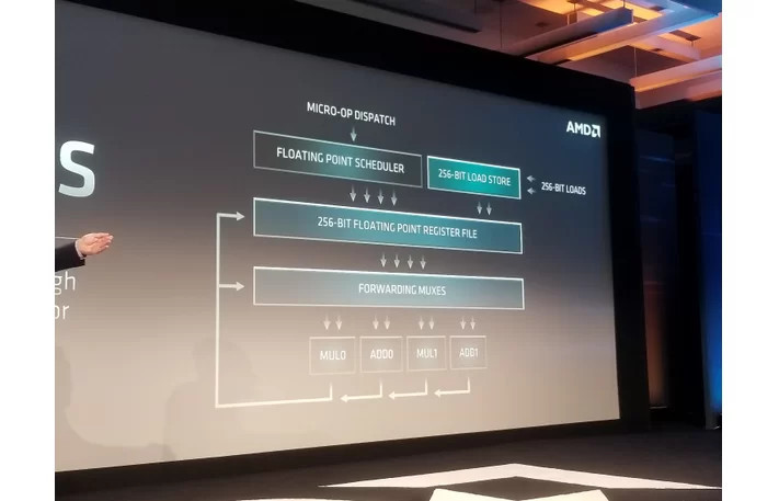
According to Expreview, AMD conducted DKERN + RSA test for integer and floating point units, to arrive at a performance index of 4.53, compared to 3.5 of first-generation Zen, which is a 29.4 percent IPC uplift (loosely interchangeable with single-core performance). "Zen 2" goes a step beyond "Zen+," with its designers turning their attention to critical components that contribute significantly toward IPC - the core's front-end, and the number-crunching machinery, FPU. The front-end of "Zen" and "Zen+" cores are believed to be refinements of previous-generation architectures such as "Excavator." Zen 2 gets a brand-new front-end that's better optimized to distribute and collect workloads between the various on-die components of the core. The number-crunching machinery gets bolstered by 256-bit FPUs, and generally wider execution pipelines and windows. These come together yielding the IPC uplift. "Zen 2" will get its first commercial outing with AMD's 2nd generation EPYC "Rome" 64-core enterprise processors.

Update Nov 14: AMD has issued the following statement regarding these claims.
Source:
Expreview
According to Expreview, AMD conducted DKERN + RSA test for integer and floating point units, to arrive at a performance index of 4.53, compared to 3.5 of first-generation Zen, which is a 29.4 percent IPC uplift (loosely interchangeable with single-core performance). "Zen 2" goes a step beyond "Zen+," with its designers turning their attention to critical components that contribute significantly toward IPC - the core's front-end, and the number-crunching machinery, FPU. The front-end of "Zen" and "Zen+" cores are believed to be refinements of previous-generation architectures such as "Excavator." Zen 2 gets a brand-new front-end that's better optimized to distribute and collect workloads between the various on-die components of the core. The number-crunching machinery gets bolstered by 256-bit FPUs, and generally wider execution pipelines and windows. These come together yielding the IPC uplift. "Zen 2" will get its first commercial outing with AMD's 2nd generation EPYC "Rome" 64-core enterprise processors.

As we demonstrated at our Next Horizon event last week, our next-generation AMD EPYC server processor based on the new 'Zen 2' core delivers significant performance improvements as a result of both architectural advances and 7nm process technology. Some news media interpreted a 'Zen 2' comment in the press release footnotes to be a specific IPC uplift claim. The data in the footnote represented the performance improvement in a microbenchmark for a specific financial services workload which benefits from both integer and floating point performance improvements and is not intended to quantify the IPC increase a user should expect to see across a wide range of applications. We will provide additional details on 'Zen 2' IPC improvements, and more importantly how the combination of our next-generation architecture and advanced 7nm process technology deliver more performance per socket, when the products launch.
162 Comments on AMD "Zen 2" IPC 29 Percent Higher than "Zen"
CFL is ahead of Zen (1) and Zen 2 will probably close that gap, yes. Hopefully not just IPC but also clocks.
Intel should do a lot of things, but the reality is they have nothing on the table unless they can move to a smaller node.
For the source of this info ->
www.techspot.com/article/1616-4ghz-ryzen-2nd-gen-vs-core-8th-gen/
(And yes, I'm aware there are specific scenarios where the IPC gap can be noticeable, but I'm talking about the average usecase here).
Intel at a point was in the lead with 2 manufacturing steps.
Now Intel has nothing to answer this with and is behind in every aspect except marketing dirty tricks (oh... 'deals').
Now, let's look at that sketch. In it, any given CCX is one hop away from 3-4 other CCXes, 2 hops from 3-5 CCXes, and 3 hops away from the remaining 7-10 CCXes. In comparison, with EPYC (non-Rome) and TR, all cores are 1 hop away from each other (though the inter-CCX hop is shorter/faster than the die-to-die IF hop). Even if this is "reduced latency IF" as they call it, that would be ridiculous. And again: what role does the I/O die play in this? The IF layout in that sketch makes no use of it whatsoever, other than linking the memory controller and PCIe lanes to eight seemingly random CCXes. This would make NUMA management an impossible flustercuck on the software side, and substrate manufacturing (seriously, there are six IF links in between each chiplet there! The chiplets are <100mm2! This is a PCB, not an interposer! You can't get that kind of trace density in a PCB.) impossible on the hardware side. Then there's the issue of this design requiring each CCX to have 4 IF links, but 1/4 of the CCXes only gets to use 3 links, wasting die area.
On the other hand, let's look at the layout that makes sense both logically, hardware and software wise, and adds up with what AMD has said about EPYC: Each chiplet has a single IF interface, that connects to the I/O die. Only that, nothing more. The I/O die has a ring bus or similar interconnect that encompasses the 8 necessary IF links for the chiplets, an additional 8 for PCIe/external IF, and the memory controllers. This reduces the number of IF links running through the substrate from 30 in your sketch (6 per chiplet pair + 6 between them) to 8. It is blatantly obvious that the I/O die has been made specifically to make this possible. This would make every single core 1 hop (through the I/O die, but ultimately still 1 hop) away from any other core, while reducing the number of IF links by almot 1/4. Why else would they design that massive die?
Red lines. The I/O die handles low-latency shuffling of data between IF links, while also giving each chiplet "direct" access to DRAM and PCIe. All over the same single connection per chiplet. The I/O die is (at least at this time) a black box, so we don't know whether it uses some sort of ring bus, mesh topology, or large L4 cache (or some other solution) to connect these various components. But we do know that a layout like this is the only one that would actually work. (And yes, I know that my lines don't add up in terms of where the IF link is physically located on the chiplets. This is an illustration, not a technical drawing.)
More on-topic, we need to remember that IPC is workload dependent. There might be a 29% increase in IPC in certain workloads, but generally, when we talk about IPC it is average IPC across a wide selection of workloads. This also applies when running test suites like SPEC or GeekBench, as they run a wide variety of tests stressing various parts of the core. What AMD has "presented" (it was in a footnote, it's not like they're using this for marketing) is from two specific workloads. This means that a) this can very likely be true, particularly if the workloads are FP-heavy, and b) this is very likely not representative of total average IPC across most end-user-relevant test suites. In other words, this can be both true (in the specific scenarios in question) and misleading (if read as "average IPC over a broad range of workloads").
- Two 8-core chiplets with a smaller I/O die that has 2-channel memory, 32-lane PCIe gen 4.0 (with external redrivers), and the same I/O as current AM4 dies such as ZP or PiR.
- A monolithic die with two 8-core CCX's, and fully integrated chipset like ZP or PiR. Such a die wouldn't be any bigger than today's PiR.
I think option two is more feasible for low-margin AM4 products.But let's wait and see.
It's somewhat like the USA-PRC military equation. For every dollar that China spends on developing a new military technology, the US probably spends $5 to keep its edge (thanks to lubricating K-street, the hill, MIC, higher costs, etc.).
There's the IPC, and then there's IPS.
IPC or I/c → Instructions per (Clock-) Cycle
IPS or I/s → Instructions per Second
The letter one, thus IPS, often is used synonymously with and for actual Single-thread-Performance – whereas AMD no longer and surely not to such an extent lags behind in numbers compared to Intel now as they did at the time Bulldozer was the pinnacle of the ridge.
Rule of thumb:
IPC does not scale with frequency but is rather fix·ed (within margins, depends on context and kind of [code-] instructions¹, you got the idea).
IPS is the fixed value of the IPC in a time-relation or at a time-figure pretty much like the formula → [ICODE]IPC×t[/ICODE], simply put.
So your definition of IPC quoted above would rather be called „Instructions per Clock at the Wall“ like IPC@W.
So please, stop using right terms and definitions for wrong contexts, learn the difference between those two and get your shit together please!
¹ The value IPC is (depending on kind) absolute² and fixed, yes.
However, it completely is crucially depending on the type and kind of instructions and can vary rather stark by using different kind of instructions – since, per definition, the figure IPC only reflects the value of how many instructions can be processed on average per (clock-) circle.
On synthetic code like instructions with low logical depth or level and algorithmic complexity, which are suited to be processed rather shortly, the resulting value is obviously pretty high – whereas on instructions with a rather high complexity and long length, the IPC-value can only reach rather low figures. In this particular matter, even the contrary can be the case, so that it needs more than one or even a multitude of cycles to process a single given complex instruction. In this regard we're speaking of the reciprocal multiplicative, thus the inverse (-value).
… which is also standardised as being defined as (Clock-) Cycles per Instruction or C/I, short → CPI.
² In terms of non-varying, as opposed to relative.
Read:
Wikipedia • Instructions per cycle
Wikipedia • Instructions per second
Wikipedia • Cycles per instruction
Smartcom
Eh... IPS in my mind is In Plane Switching for displays.
He spelled it fine, you didn't read it right.