Monday, November 12th 2018

AMD "Zen 2" IPC 29 Percent Higher than "Zen"
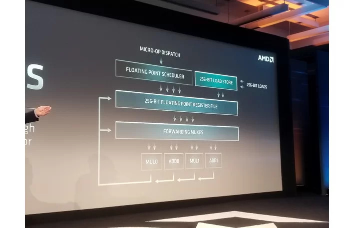
AMD reportedly put out its IPC (instructions per clock) performance guidance for its upcoming "Zen 2" micro-architecture in a version of its Next Horizon investor meeting, and the numbers are staggering. The next-generation CPU architecture provides a massive 29 percent IPC uplift over the original "Zen" architecture. While not developed for the enterprise segment, the stopgap "Zen+" architecture brought about 3-5 percent IPC uplifts over "Zen" on the backs of faster on-die caches and improved Precision Boost algorithms. "Zen 2" is being developed for the 7 nm silicon fabrication process, and on the "Rome" MCM, is part of the 8-core chiplets that aren't subdivided into CCX (8 cores per CCX).
According to Expreview, AMD conducted DKERN + RSA test for integer and floating point units, to arrive at a performance index of 4.53, compared to 3.5 of first-generation Zen, which is a 29.4 percent IPC uplift (loosely interchangeable with single-core performance). "Zen 2" goes a step beyond "Zen+," with its designers turning their attention to critical components that contribute significantly toward IPC - the core's front-end, and the number-crunching machinery, FPU. The front-end of "Zen" and "Zen+" cores are believed to be refinements of previous-generation architectures such as "Excavator." Zen 2 gets a brand-new front-end that's better optimized to distribute and collect workloads between the various on-die components of the core. The number-crunching machinery gets bolstered by 256-bit FPUs, and generally wider execution pipelines and windows. These come together yielding the IPC uplift. "Zen 2" will get its first commercial outing with AMD's 2nd generation EPYC "Rome" 64-core enterprise processors.

Update Nov 14: AMD has issued the following statement regarding these claims.
Source:
Expreview
According to Expreview, AMD conducted DKERN + RSA test for integer and floating point units, to arrive at a performance index of 4.53, compared to 3.5 of first-generation Zen, which is a 29.4 percent IPC uplift (loosely interchangeable with single-core performance). "Zen 2" goes a step beyond "Zen+," with its designers turning their attention to critical components that contribute significantly toward IPC - the core's front-end, and the number-crunching machinery, FPU. The front-end of "Zen" and "Zen+" cores are believed to be refinements of previous-generation architectures such as "Excavator." Zen 2 gets a brand-new front-end that's better optimized to distribute and collect workloads between the various on-die components of the core. The number-crunching machinery gets bolstered by 256-bit FPUs, and generally wider execution pipelines and windows. These come together yielding the IPC uplift. "Zen 2" will get its first commercial outing with AMD's 2nd generation EPYC "Rome" 64-core enterprise processors.

As we demonstrated at our Next Horizon event last week, our next-generation AMD EPYC server processor based on the new 'Zen 2' core delivers significant performance improvements as a result of both architectural advances and 7nm process technology. Some news media interpreted a 'Zen 2' comment in the press release footnotes to be a specific IPC uplift claim. The data in the footnote represented the performance improvement in a microbenchmark for a specific financial services workload which benefits from both integer and floating point performance improvements and is not intended to quantify the IPC increase a user should expect to see across a wide range of applications. We will provide additional details on 'Zen 2' IPC improvements, and more importantly how the combination of our next-generation architecture and advanced 7nm process technology deliver more performance per socket, when the products launch.
162 Comments on AMD "Zen 2" IPC 29 Percent Higher than "Zen"
Not to mention that the clock speeds are unknown. They have to be completely fixed to benchmark anything close to IPC.Games are in fact one of the workloads that is the least superscalar and have the most branch and cache mispredictions. The reason why AMD scale well for certain superscalar workloads (like Blender and certain encoding and compression tasks) is that Zen have more "brute force" through ALUs/FPUs on execution ports, but fall short in gaming due a weaker front-end/prefetcher. Intel have few execution ports but achieve higher efficiency through better prediction and caching.
Bottom line, I just don't see a problem here. Clearly everyone into tech can figure out how to run these CPUs. And those who can't aren't probably spending the money on these. All I see here is a (typical by now) "omg! Intel did X, they're screwing end users!!!" reaction. When CPUs get this complex, specs get this complex too, that's all there is to it.
From what I can see from reviews, without AVX 9900K actually does consume close enough to the rated 95W.
That is also something we can look forward to analyzing in Zen2.You would think it is that simple and straightforward especially with the perfect power management (at least on the package level) on Ryzens. I have a 2400G on that same Gigabyte board that most reviewers got. It used to have cTDP option in the BIOS but that went missing after a BIOS update. Similarly, the damn board actually had an MCE-like setting that indeed used to run my poor 2400G at 95-100W.
Ryzen uses the FPU as a coprocessor, so there's a good chunk of delay from when instructions are decoded and when they are executed... and dependent integer or memory operations are processed in parallel as far as possible. This isn't strictly superscalar simply because the execution steps become disjointed after classification as floating point, memory, or integer, and the front end generates multiple instruction streams from a single instruction stream.
That wasn't so hard, now was it?
dkern can be extremely useful for testing the front end... but you need to have a rather large vector upon which to operate for that to happen... and we just don't know what AMD was doing with dkern since it's just a function that operates on data. However, dkern has branches, does integer or floating point comparisons, decrements, subtraction, division, and operates on potentially large amounts of data (usually image or scientific data, being a statistical smoothing method).
RSA in this situation could be used to decrypt or encrypt the data being accessed or could be an entirely other program being used... or AMD ran two benchmarks and averaged the results... they were very unclear.
RSA has a few tight loops, multiplication, division, comparisons and branches within loops, and potentially significant bandwidth utilization (simply jumping to L2 counts as significant in this context).They are usually bottlenecked by ALU->FPU communication or, as you say, cache miss penalties. Ryzen's sequential cache performance is very good, but it falls flat with random accesses, so that is definitely a significant role - and hopefully something AMD has resolved with Zen 2. A 33% improvement in ALU->FPU throughput means ~10% improvement for many CPU bottlenecked games per cycle. That puts them roughly on par with Intel for those games. Others that are thrashing the cache (which would be a bad game engine - of which there are plenty (I'm looking at you Hitman!)) won't care at all about that improvement (or very little... or even "dislike" it). Here, of course, Zen 2 will need to have reduced semi-random access latencies. It doesn't help that each core advertises access to 8MiB of L3 but only seems to search 4MiB worth of tags before jumping to the IMC. An L4 would help here - we wouldn't be hitting memory latencies for in-page random access, in the very least, but would be much closer to Intel's ~20ns figures.
Cache is organized in banks. Zen's 8-way 512kB L2 is actually 8 separate 64kB caches (Skylake have 4-way 256kB, Haswell 8-way 256kB). Memory is stored in 64b cache lines, for sequential reads the cache lines will be evenly spread across the banks. Zen having 8×64kB L2 caches vs. Skylake's 4x64kB caches should not give Zen any disadvantage in latency or throughput.
Intel's advantage isn't a faster cache, it's a better front-end/prefetcher to detect linear accesses which improves cache hit ratio.
What does random accesses have to do with this? Nothing can ever predict random accesses, they will fall through the cache and read directly from memory. The only thing that can marginally help here is the OoOE trying to dereference a pointer etc. as early as possible, but usually the limits to how far ahead the prefetcher can "see", and of course all branching logic and other pointers may limit the room for early execution here. Once again this has to do with the efficiency of the prediction, not the latency of the cache.You mean that each four cores shares one L3 cache?
L3 cache is largely a "spillover cache", cache lines which have been recently used but kicked out of L2. Even in heavy multithreaded workloads, very little L3 is ever shared among cores. And when it is, it's mostly code, not data. When it comes to writing, the CPU engages a write-lock to discard a cache line from all caches, any latency here comes down to the entire memory structure, not the L3.
I also want to remind you that Intel switched their memory structure in Skylake-X/-SP vs. Skylake, making L2 larger and L3 smaller, but making L3 exclusive, and they improved overall efficiency.
I don't see any evidence to support that Zen is disadvantaged from having 4MB L3 per core. If they add an L4, it will basically be a larger "spillover cache", and they would also have to be careful not to increase overall latency by the added complexity.
It can be a little easy to forget that Zen's FPU is a dedicated unit that has to have specific points of communication with the integer+memory complex whereas Intel's floating point units are on the same pipelines as their integer units.Ideally, yes, you should never have a stall with streaming data... but there's a difference between operating with data right off a data bus, within the register file, hitting the 1ns latency of L1D, or hitting the 3~4ns latency of the L2. On Zen, at least, there's no real bandwidth penalty for hitting the L2.That's not the issue... the L2 is really good... it's when we get inside the L3 that issues begin... and they explode once we hit the IMC.
Games, for their part, often do a pretty good job of imitating a random memory access pattern... which is why Ryzen's game performance can jump 15% or more with overclocked memory. Give Zen the same memory latency as Intel cores have and I think the Ryzen 2700X would be the gaming king per clock.Data sharing is insanely common in multi-threaded programs. If it wasn't we wouldn't have to worry so much about lock contention. I have a good ~20 years of MT programming experience (from way back in the BeOS 4.5 era) with numerous programming languages, operating systems, and devices. I directly tested Zen's inter-core and inter-CCX communications to discover that there was a fast-path (low latency, low bandwidth) communication path for small data packets before AMD detailed the command fabric. I discovered it by accident because I couldn't explain how I was getting data between Core 0 to Core7 (on different CCXes) with only something like a 20ns penalty versus going from core 0 to core 1 (same CCX, neighboring cores).... but I digress...Yes, they copied Zen (kind of a joke...). Though AMD uses a 'mostly' exclusive design - though we don't fully know, AFAIK, what they mean by that.It's not the 4MiB per core - it's what happens in many scenarios when a core tries to access beyond that basic block...
On Intel CPUs there are games where faster memory benefits but this is far from common and in many cases memory speed makes a negligible difference. The same does not apply to Ryzens, these will get a jump from faster memory across the board.
What you're forgetting though is that without these "best case" benches there would be little to no IPC gain, for Intel, in the last few years. Take the FP numbers out, heavily influenced by AVX2 or AVX512, & you have virtually 0 IPC gains for close to 4 years, if not more. That's because x86 has pretty much reached the end of the line so far as IPC gains are concerned. The biggest performance gains this decade have come from tweaking cache hierarchy, DDR4, AVX & clock speeds. That's not the case for ARM but it's also not a part of this debate.
Why do I see this dismissive tone when talking about ARM here, do you buy phones with Intel Inside? Why do you think that is, do you treat (one of) AMD vs Nvidia the same way?
The other part is why are you dismissive about x86? There have been some tests on single core performance here and there from Sandy Bridge forward (7 years). For example:
m.sweclockers.com/test/23426-amd-ryzen-7-1800x-och-7-1700x/29
23% in Cinebench is not too bad. And Cinebench does only 128-bit AVX (which is from Sandy Bridge/Bulldozer era).
Intel has been stuck on Skylake and derivatives for 3 years but I would not necessarily put this down to inability to improve IPC. Core count is the clear focus for the last few years.
I've also noted that the biggest changes have been in cache, memory, clock speeds & arguably HT or SMT for AMD. Admittedly ARM also benefits from that, but again the point is ARM are coming from a much smaller base (number) & so their gains are incredible. The biggest servers, supercomputers will still be vastly x86 based, but as you've said that's down to more cores. IMO (chip) interconnect technologies like UPI or IF are the next & perhaps the last hurdle before x86 reaches it's peak. I don't see the same kind of progress in the next decade, as we've seen since 2010 unless there's some major breakthrough. The future is dedicated (hardware) accelerators, that is where I see computing realm headed. The core wars have just begun but even there physics will catch up pretty soon.
Memory speeds have increased, yes. Well, latency not so much but bandwidth for sure. Memory improvement will continue. DDR5 is on its way and for some implementations, GDDR/HBM with their respective up- and downsides. How much this affects results depends on benchmark. In case of Cinebench, it has a very low scaling with faster memory.
The Cinebench test I linked is at the same clock speeds and single core/thread so no HT/SMP in play.I do not know if I would want to separate FP from general CPU performance. FP has been a part of x86 for a long time - in coprocessors since the beginning, integrated in and Pentium onwards. Improving parts of the instruction set is part of CPU evolution.Comparisons with ARM are difficult. In addition to integrating performance-improving aspects (many of them tried-and-true) ARM has been moving to scale its architecture(s) higher and higher, largely funded and driven by smartphones. Higher-performing ARM CPUs are not small and they do consume considerable amounts of power.
Actually, since you mentioned AVX and other instruction-level improvements being a bit suspect when comparing IPC, ARM has gained a lot of its IPC and almost all of its FP performance from just that. Since ARM's focus is different, they are also going for more cores rather than more performance, especially in the last few years. They also benefit from not having to be compatible :)
Rest of your post I wholeheartely agree with.
AMD have clarified in the meantime 29% was based on one particular benchmark. So we're basically back to square one.
From what we know, the breakdown in performance improvements. for this workload, probably looks something such as this:
- Fetch: . . . . . . 0-5% . . . . . . . .(from L2/L3/IMC)
- Dispatch: . . . 30~35% . . . . . (next instruction counter, larger uop cache, wider dispatch width)
- ALU: . . . . . . . 5-15% . . . . . . . (instructions in play are all too simple to see much improvement, so this would be the predictor improvement as it relates to these simple tests)
- FPU: . . . . . . . 15-33% . . . . . . (non-AVX workload, advantage comes from load bandwidth doubling).
- Retire: . . . . . .70~80% . . . . . .(from doubling of retirement bandwidth - 128-bit to 256-bit - not 100% because of naturally imperfect scaling)
These values would average together to become the IPC increase for this particular workload. These should be the ranges to expect for any program going through the CPU... with some major caveats - such as the fetch and ALU performance not being well represented in this workload - and the dispatch and retire ruling the day.___________________
Also, x86 has plenty of room for improvement. We just have to start walking away from relative energy efficiency.
If we had a process that allowed us to execute and fetch memory with almost no power usage, we would easily double IPC. Everything in a modern CPU is a compromise for power efficiency... including how aggressively you do predictive computation.
Heck, if we created a semi-dedicated pipeline for predictions and left another dedicated path for in-order execution (leaving instruction bubbles and all, but with power gating), we would see cache miss penalties drop close to zero as we could execute both possibilities for a branch outcome then just move over each stage results after a branch prediction is shown true - removing the instruction bubble with a single cycle latency and resulting in nearly perfect prediction performance. This is insane in the world where power consumption is important... you will be executing (partly or in full) nearly every instruction in a program - even for branches not taken... we're talking about potentially more than doubling how much is executed for every clock cycle. Still, this would be something like a 50% IPC increase.