Monday, November 12th 2018

AMD "Zen 2" IPC 29 Percent Higher than "Zen"

AMD reportedly put out its IPC (instructions per clock) performance guidance for its upcoming "Zen 2" micro-architecture in a version of its Next Horizon investor meeting, and the numbers are staggering. The next-generation CPU architecture provides a massive 29 percent IPC uplift over the original "Zen" architecture. While not developed for the enterprise segment, the stopgap "Zen+" architecture brought about 3-5 percent IPC uplifts over "Zen" on the backs of faster on-die caches and improved Precision Boost algorithms. "Zen 2" is being developed for the 7 nm silicon fabrication process, and on the "Rome" MCM, is part of the 8-core chiplets that aren't subdivided into CCX (8 cores per CCX).

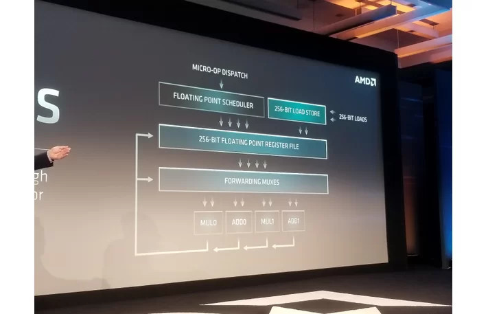
According to Expreview, AMD conducted DKERN + RSA test for integer and floating point units, to arrive at a performance index of 4.53, compared to 3.5 of first-generation Zen, which is a 29.4 percent IPC uplift (loosely interchangeable with single-core performance). "Zen 2" goes a step beyond "Zen+," with its designers turning their attention to critical components that contribute significantly toward IPC - the core's front-end, and the number-crunching machinery, FPU. The front-end of "Zen" and "Zen+" cores are believed to be refinements of previous-generation architectures such as "Excavator." Zen 2 gets a brand-new front-end that's better optimized to distribute and collect workloads between the various on-die components of the core. The number-crunching machinery gets bolstered by 256-bit FPUs, and generally wider execution pipelines and windows. These come together yielding the IPC uplift. "Zen 2" will get its first commercial outing with AMD's 2nd generation EPYC "Rome" 64-core enterprise processors.

Update Nov 14: AMD has issued the following statement regarding these claims.
As we demonstrated at our Next Horizon event last week, our next-generation AMD EPYC server processor based on the new 'Zen 2' core delivers significant performance improvements as a result of both architectural advances and 7nm process technology. Some news media interpreted a 'Zen 2' comment in the press release footnotes to be a specific IPC uplift claim. The data in the footnote represented the performance improvement in a microbenchmark for a specific financial services workload which benefits from both integer and floating point performance improvements and is not intended to quantify the IPC increase a user should expect to see across a wide range of applications. We will provide additional details on 'Zen 2' IPC improvements, and more importantly how the combination of our next-generation architecture and advanced 7nm process technology deliver more performance per socket, when the products launch.
Source: Expreview
Add your own comment

162 Comments on AMD "Zen 2" IPC 29 Percent Higher than "Zen"

#101
looncraz
BlueberriesZen 2 won't have anywhere near 29% more IPC, I'd have to be smoking some funny stuff to believe that again.
On average? Absolutely not - that would be insane. But for areas where Zen is currently weak? Quite possible.

Even the scenario AMD showed had to have two concurrent loads to see 29%. But that's another side of CPU performance many don't think about - loaded performance.

This should translate well into SMT scaling.
Posted on Reply
#102
CheapMeat
Most of you guys are writing as if you're buying EPYC. I bet 99% of you are NOT. The speculation here is all what has been presented for EPYC, especially the way the package is. There's no confirmation on what Ryzen will be exactly and how it'll be packaged. Lets just be honest here about what you are all actually buying and/or willing to spend money on.
Posted on Reply
#103
Smartcom5
bugWell, I don't see it as deceptive, because 95W is all a board manufacturer has to support.
But when you start using words like "without question" to make your point, you're kind of preventing us further discussing this. Have a nice day.
Well, I thought so …
If you put that CPU on a board which has vrm-phases designed to support such an CPU with a power-draw of up to said 95W of total drawn power, the 9900K is a overpriced piece of hot garbage.
The pseudo-argument of that excuse that K-CPUs of such kind wouldn't be used on such boards is irrelevant as this CPU is explicitly marketed with that 95W on purpose to trick people into believing exactly that, so that it actually draws up to said 95W (which isn't the case at all) – not at stock nor on any default BIOS/UEFI-settings boards get shipped with et cetera.

Though if you have any greater trouble figuring out the bare condition if an marketing-campaign for a device, which is advertised with only 95W of power-draw – which it actually overdraws significantly 90% of the time it's active – shall be be deceitful or not, I don't know what to tell you. You don't seem to get the point at all – either on purpose (which pretty much seems to be the actual case here, given your kind of arguing) or due to a fundamental lack of moral understanding and ethical perception (which actually shall be considered being the required condition to defend such practices in the first place).

You too may have a nice day!


Smartcom
Posted on Reply
#104
Arjai
Intel-er's will be Intel-er's.

RyZen has been amazing, since day one. Unlike Intel, It HAS been getting better( kind of like how the Vega cards have incrementally, moved up the ranks). AMD, if anyone remembers, did kick Intel's butt. It has been a while but, disbelieving it could happen again? Simply, childish.

I don't know the chain of command in Intel but, AMD? Lisa. Can anyone provide proof, that she is a liar?

I am going to buy stock in AMD, 2 days from now. See you when I am rich-er! :lovetpu:
Posted on Reply
#105
looncraz
CheapMeatMost of you guys are writing as if you're buying EPYC. I bet 99% of you are NOT. The speculation here is all what has been presented for EPYC, especially the way the package is. There's no confirmation on what Ryzen will be exactly and how it'll be packaged. Lets just be honest here about what you are all actually buying and/or willing to spend money on.
I doubt many of us will buy EPYC 2, but that's why we're talking about the core itself - it's independent of what SKU we're talking about.

Ryzen 3000 could come with nothing smaller than a six core CPU (I hope AMD does this - Intel could barely adapt last time when quad core became the new low end mainstream CPU).


AMD gets 800~900 usable chiplets per 7nm wafer. Assuming a $12k wafer cost (which is close) and a relatively high defect rate of 0.3/cm^2, that's just $14 per chiplet. Two of those and a $10 IO die and you have a quite similar bill of material as Ryzen originally did on launch... except now AMD has 16 cores on the mainstream desktop and can happily ask $600 for it. And I'd pay it.
Posted on Reply
#106
HTC
looncrazI doubt many of us will buy EPYC 2, but that's why we're talking about the core itself - it's independent of what SKU we're talking about.

Ryzen 3000 could come with nothing smaller than a six core CPU (I hope AMD does this - Intel could barely adapt last time when quad core became the new low end mainstream CPU).


AMD gets 800~900 usable chiplets per 7nm wafer. Assuming a $12k wafer cost (which is close) and a relatively high defect rate of 0.3/cm^2, that's just $14 per chiplet. Two of those and a $10 IO die and you have a quite similar bill of material as Ryzen originally did on launch... except now AMD has 16 cores on the mainstream desktop and can happily ask $600 for it. And I'd pay it.
You're not taking into account the fact 7 nm process isn't mature yet, dude. Also, isn't the wafer size supposed to be 300 mm?

According to this:


I chose a defect density of 0.4 because it's a new process, and with these parameters, AMD would get 612 good dies. Note the die dimensions are rounded down (from 73 mm²) to make the calculations a tad bit easier.

Here's the link for the Die Per Wafer Calculator: caly-technologies.com/die-yield-calculator/
Posted on Reply
#107
R0H1T
We don't know the defect rate so any speculation wrt same is pointless, what's more relevant though is the price these chips command in the server space or high end retail. The price of dies is rather low, so that's not much of a problem anyway.
Posted on Reply
#108
looncraz
HTCYou're not taking into account the fact 7 nm process isn't mature yet, dude. Also, isn't the wafer size supposed to be 300 mm?

According to this:


I chose a defect density of 0.4 because it's a new process, and with these parameters, AMD would get 612 good dies. Note the die dimensions are rounded down (from 73 mm²) to make the calculations a tad bit easier.

Here's the link for the Die Per Wafer Calculator: caly-technologies.com/die-yield-calculator/
Yes, 300mm wafer, 0.12mm scribe, 5mm edge loss. The absense of a DFZ parameter is unfortunate (the stepback distance from a cut edge to avoid defects in the circuitry).

Also, when these things say "good" dies, they mean "perfect" dies. A defective die may only have a bad core or some other minor, recoverable, fault, so "max dies" is the upper bound, so your numbers are 612~812 using a larger, square, die. The shape plays a relatively minor role at this size, but it can play a more prominent role as the die grows, so keep that in mind, as the height of the chiplet is 1.4X greater than the width.

0.4 would be rather bad. 14nm had 0.08 at launch, I seriously doubt 7nm HPC has anything notably higher than 0.3 - and probably closer to 0.2 or even below. I based my numbers on a range from 0.2 to 0.3 (which I probably should have stated in my comment).

6.75x9.45mm = 63.79mm^2 = 731~938 usable dies with a 0.4 defect density and 0.12 scribe h+V lanes.

Move to 0.3 defects/cm^2 and you have 827~938 usable dies.
R0H1TWe don't know the defect rate so any speculation wrt same is pointless, what's more relevant though is the price these chips command in the server space or high end retail. The price of dies is rather low, so that's not much of a problem anyway.
Well, a $20 chiplet would dictate that Ryzen can only really afford to have one chiplet without having two designs - one with one chiplet and another with two.

$20 represents ~600 usable dies per wafer. A silicon bill of materials in excess of $50 for Ryzen's core would be a big jump... and a big risk to bring to the mainstream market.

At $12 per chiplet - a price that will decline with time - AMD can toss two chiplets onto every Ryzen CPU, with a BoM pretty close to Ryzen's original costs.
Posted on Reply
#109
R0H1T
looncrazWell, a $20 chiplet would dictate that Ryzen can only really afford to have one chiplet without having two designs - one with one chiplet and another with two.

$20 represents ~600 usable dies per wafer. A silicon bill of materials in excess of $50 for Ryzen's core would be a big jump... and a big risk to bring to the mainstream market.

At $12 per chiplet - a price that will decline with time - AMD can toss two chiplets onto every Ryzen CPU, with a BoM pretty close to Ryzen's original costs.
The headline number, for me, is the usable dies ~ which directly translates into lower/higher cost (per die) depending on defect rate. The number of usable dies is really important because it helps AMD keep up with their scheduled timelines, launch dates, demand & commitment especially towards large customers. It is said (by some) that AMD sold every chip they could produce in the Intel OEM bribing era, I can't say how true that is but AMD atm absolutely needs to fulfill the demand for Rome & compete for the growing needs of enterprise sector. Which is to say that the cost of dies is secondary, but again directly related to defect rate, right now while meeting obligations should be the primary goal, especially the Super 7 plus one.
Posted on Reply
#110
HTC
looncraz0.4 would be rather bad. 14nm had 0.08 at launch, I seriously doubt 7nm HPC has anything notably higher than 0.3 - and probably closer to 0.2 or even below. I based my numbers on a range from 0.2 to 0.3 (which I probably should have stated in my comment).

6.75x9.45mm = 63.79mm^2 = 731~938 usable dies with a 0.4 defect density and 0.12 scribe h+V lanes.

Move to 0.3 defects/cm^2 and you have 827~938 usable dies.
Are you referring to the 1st chip on 14 nm or to the 1st Zen chip on 14 nm? IIRC, when Zen was introduced, there were several chips being manufactured @ 14 nm, meaning the process was much more mature then 7 nm, where it is the 2nd chip (1st is Apple's A12 chip).

What is your source of Zen 2 CCX chiplet size? From what i've read, Zen 2 CCX chiplet measurement is roughly 73 mm² while yours is almost 10 mm² smaller.

For reference, i got those measurements from this post @ Anandtech forums.

When i made the pic in my previous reply, i was under the impression the CCX chiplet size was 72 mm² and that the chiplet was a square instead of a rectangle.

According to the die calculator page, those scribe values are invalid: either 0.1 or 0.15 but not 0.12.

Base on the current information, and with a defect density of 0.25, we get this (7.3 is also an invalid number for width so i improvised):

Posted on Reply
#111
R0H1T
HTCAre you referring to the 1st chip on 14 nm or to the 1st Zen chip on 14 nm? IIRC, when Zen was introduced, there were several chips being manufactured @ 14 nm, meaning the process was much more mature then 7 nm, where it is the 2nd chip (1st is Apple's A12 chip).

What is your source of Zen 2 CCX chiplet size? From what i've read, Zen 2 CCX chiplet measurement is roughly 73 mm² while yours is almost 10 mm² smaller.

For reference, i got those measurements from this post @ Anandtech forums.

When i made the pic in my previous reply, i was under the impression the CCX chiplet size was 72 mm² and that the chiplet was a square instead of a rectangle.

According to the die calculator page, those scribe values are invalid: either 0.1 or 0.15 but not 0.12.

Base on the current information, and with a defect density of 0.25, we get this (7.3 is also an invalid number for width so i improvised):

No Zen was the first high performance chip using GF 14nm, you could count Polaris but that's not exactly apples to apples.
Posted on Reply
#112
HTC
R0H1TNo Zen was the first high performance chip using GF 14nm, you could count Polaris but that's not exactly apples to apples.
Only Polaris? I thought there were others: i'm probably miss remembering :(

Correct me if i'm wrong but a process is independent from the chips, no? If so, then the experience from the Polaris chips helped with Zen by making the process more mature, thus making the defect density smaller, no?
Posted on Reply
#113
GoldenX
BlueberriesZen 2 won't have anywhere near 29% more IPC, I'd have to be smoking some funny stuff to believe that again.
Nobody believed that Zen1 was 59% better than FX.
I'm happy with a 15% increase plus clock speed increase.
Posted on Reply
#114
Legacy-ZA
If AMD keeps their prices very competitive like they are now, I will be upgrading to Zen 2.
Posted on Reply
#115
Valantar
WikiFMSo a cheap 8121U has AVX512 and also the $359 7800X 14 nm, so mainstream AVX512 is a reality that could have been widely spread by now.
The 8121U has its AVX512 units (as well as pretty much everything else) disabled.
CheapMeatMost of you guys are writing as if you're buying EPYC. I bet 99% of you are NOT. The speculation here is all what has been presented for EPYC, especially the way the package is. There's no confirmation on what Ryzen will be exactly and how it'll be packaged. Lets just be honest here about what you are all actually buying and/or willing to spend money on.
None of us will be buying EPYC. That's why we're taking what they've said about it and attempting to extrapolate what this means for Ryzen 3000 and TR3. Also, it's interesting to discuss when someone makes some actual innovations in this space, even if we're not in the target market.
Legacy-ZAIf AMD keeps their prices very competitive like they are now, I will be upgrading to Zen 2.
I'd actually consider the same, even if I'm very happy with my 1600X.
Posted on Reply
#116
Aquinus
Resident Wat-man
WikiFMSo what gives better yields then? Smaller dies at 7nm or a huge one at 14nm? Yes the I/O die is done in GloFo's 14 nm.
nemesis.ie@Aquinus It was confirmed at the NH event that the I/O chip is on 14nm.

My guess is that it could be from GF which keeps GF in the game.
Both actually. Smaller 7nm dies for the CCXs will help yields for a less mature process because smaller dies almost always translates to more usable dies. The larger I/O chip benefits from the maturity of the 14nm process which is likely to have better yields for larger dies which keeps costs down. This is actually the reason why Intel's PCHs are on a larger process than the node the CPUs are made on. It's really all about costs and yields because some components don't need to be on the smaller process.
AssimilatorTBH I wouldn't call the 9900K "mainstream" due to its heat, price and availability. It's pretty clearly showing the limit of the Core uarch on 14nm, and I suspect that its successor will only show up once 10nm is fixed.
Sure but, it's still on a mainstream platform so I consider it mainstream even if it's the highest end of the MSDT market.
Posted on Reply
#117
Daven
bugThis is really not complicated. More cores will draw more power, there's no bending the laws of physics. However, if you lower the base clock, you will draw less current (power does not scale linear with frequency), thus your heat sink will be cooler. When the heat sink starts cooler, it can accommodate higher frequencies for a while, until it heats up.
Again, I see no trickery at work. Just a company finding a way to squeeze more cores on a production node they were planning to leave behind at least two years ago. Both Nvidia and AMD had to do something similar when TSMC failed with their 22nm node and everybody got stuck with 28nm for a couple more years than originally planned.


Well, I don't see it as deceptive, because 95W is all a board manufacturer has to support.
But when you start using words like "without question" to make your point, you're kind of preventing us further discussing this. Have a nice day.
Anandtech does a great job with their Bench tool on their website. It helps with conversations like this one. Here are the Full package load power measurements for the last four Intel generations:
i7-6700K 82.55W
i7-7700K 95.14W
i7-8700K 150.91W
i9-9900K 168.48W
There is a major change between the 7th and 8th generations. However, Intel rates them all as 95W. You don't see a problem with this?
Source: www.anandtech.com/bench/CPU-2019/2194

EDIT: And if you look at all the CPUS at Full package load at that link, you will see almost all fall below or within +10% of the rated TDP across desktop, HEDT and server chips from both AMD and Intel. Only the 8700K and the 9900K are way off. This is deceptive advertising at its worst to try and look competitive and cover up being stuck on the same process node.
Posted on Reply
#118
Valantar
Mark LittleAnandtech does a great job with their Bench tool on their website. It helps with conversations like this one. Here are the Full package load power measurements for the last four Intel generations:
i7-6700K 82.55W
i7-7700K 95.14W
i7-8700K 150.91W
i9-9900K 168.48W
There is a major change between the 7th and 8th generations. However, Intel rates them all as 95W. You don't see a problem with this?
Source: www.anandtech.com/bench/CPU-2019/2194
I'm not who you're talking to, but I agree with the conclusion of AT's recent look into this: they should start having two numbers, one "Base TDP" and one "all-core boost TDP". That'd clear up everything quite nicely. Base TDP would indicate minimum performance specs and power delivery requirements, and all-core boost TDP would indicate what your cooler and motherboard need to match to provide the best possible out-of-box experience.
Posted on Reply
#119
Daven
ValantarI'm not who you're talking to, but I agree with the conclusion of AT's recent look into this: they should start having two numbers, one "Base TDP" and one "all-core boost TDP". That'd clear up everything quite nicely. Base TDP would indicate minimum performance specs and power delivery requirements, and all-core boost TDP would indicate what your cooler and motherboard need to match to provide the best possible out-of-box experience.
At the top of each quoted section the thread coding lists the person you are replying too. In my case, I was replying to bug. Sorry for any confusion.
Posted on Reply
#120
Valantar
Mark LittleAt the top of each quoted section the thread coding lists the person you are replying too. In my case, I was replying to bug. Sorry for any confusion.
No confusion, I just chose to reply as I more or less agree with Bug's stance :)
Posted on Reply
#121
londiste
Regarding 9900K, GamerNexus's story is probably relevant here:
www.gamersnexus.net/guides/3389-intel-tdp-investigation-9900k-violating-turbo-duration-z390
Mark LittleAnandtech does a great job with their Bench tool on their website.
Source: www.anandtech.com/bench/CPU-2019/2194
About that doing a great job - What in the world is the full load, exactly?
Edit: after clicking through some of the the linked reviews Anandtech seems to be using POV-Ray.
Posted on Reply
#122
bug
ValantarI'm not who you're talking to, but I agree with the conclusion of AT's recent look into this: they should start having two numbers, one "Base TDP" and one "all-core boost TDP". That'd clear up everything quite nicely. Base TDP would indicate minimum performance specs and power delivery requirements, and all-core boost TDP would indicate what your cooler and motherboard need to match to provide the best possible out-of-box experience.
I wouldn't mind having two numbers on the box (though as I have written above, it will certainly confuse less informed users), but which numbers would Intel use? Because only the base TDP is mandatory, the other one is left to the motherboard vendor's will.
Posted on Reply
#123
Valantar
bugI wouldn't mind having two numbers on the box (though as I have written above, it will certainly confuse less informed users), but which numbers would Intel use? Because only the base TDP is mandatory, the other one is left to the motherboard vendor's will.
Which is exactly why you call one "base" (as in "base clocks", minimum in-spec performance) and one something else. This might be a bit confusing, but no more than people buying a chip with a shitty cooler and cheap motherboard, expecting matching performance from a review, yet getting 10-20% less. Which happens quite a lot.

By making the second number official (determined by, say, the average all-core-boost power draw of the bottom 10% of chips in a specific SKU under a punishing load) Intel could make implementation uniform across motherboard vendors, with a simple "TDP" BIOS option, ("95W Base" for restricted to stock (with short-term PL2 above this) "Performance" for slightly loosened but reasonable limits, and "Unrestricted" for balls-to-the-wall?). Mainly, the second number would serve as a guideline for buying a cooler and motherboard, and it could lead to motherboard makers labeling their VRM solutions with actual useful numbers instead of "X-phase". Ultimately this could lead to less confusion, as it actually serves to explain something complex to users instead of just trying to hush it up. Intel already allows for adjusting all of this in XTU (although a lot of motherboards ignore XTU power limit settings) so why not implement it across the board? Standardisation and enforcement of standards is a boon to users, not the opposite.
Posted on Reply
#124
bug
ValantarWhich is exactly why you call one "base" (as in "base clocks", minimum in-spec performance) and one something else. This might be a bit confusing, but no more than people buying a chip with a shitty cooler and cheap motherboard, expecting matching performance from a review, yet getting 10-20% less. Which happens quite a lot.

By making the second number official (determined by, say, the average all-core-boost power draw of the bottom 10% of chips in a specific SKU under a punishing load) Intel could make implementation uniform across motherboard vendors, with a simple "TDP" BIOS option, ("95W Base" for restricted to stock (with short-term PL2 above this) "Performance" for slightly loosened but reasonable limits, and "Unrestricted" for balls-to-the-wall?). Mainly, the second number would serve as a guideline for buying a cooler and motherboard, and it could lead to motherboard makers labeling their VRM solutions with actual useful numbers instead of "X-phase". Ultimately this could lead to less confusion, as it actually serves to explain something complex to users instead of just trying to hush it up. Intel already allows for adjusting all of this in XTU (although a lot of motherboards ignore XTU power limit settings) so why not implement it across the board? Standardisation and enforcement of standards is a boon to users, not the opposite.
Oh, gee, that's so simple to explain. Try saying that to the average buyer, see how it fares :D
Posted on Reply
#125
looncraz
HTCAre you referring to the 1st chip on 14 nm or to the 1st Zen chip on 14 nm? IIRC, when Zen was introduced, there were several chips being manufactured @ 14 nm, meaning the process was much more mature then 7 nm, where it is the 2nd chip (1st is Apple's A12 chip).

What is your source of Zen 2 CCX chiplet size? From what i've read, Zen 2 CCX chiplet measurement is roughly 73 mm² while yours is almost 10 mm² smaller.

For reference, i got those measurements from this post @ Anandtech forums.

When i made the pic in my previous reply, i was under the impression the CCX chiplet size was 72 mm² and that the chiplet was a square instead of a rectangle.

According to the die calculator page, those scribe values are invalid: either 0.1 or 0.15 but not 0.12.

Base on the current information, and with a defect density of 0.25, we get this (7.3 is also an invalid number for width so i improvised):

The range is from ~64mm^2 to ~72mm^2, which is why I also include a good range in my estimates, but I focused on the smaller size since I was using it to estimate the IO die size to see how much room was left over after everything we know had to be there was inside (a healthy 120mm^2 of die space with an unknown purpose...).

I'll redo the measurements using a better image of Rome.

The 4094 package is 58.5x75.4mm. You can fit more than 10.5~10.75 width wise, giving a range from 7.01~7.18 for the width. You can fit about 5.75~6.0 height wise, giving a range of 9.75-10.17. The range is a necessity to correct for perspective (minor), pixelation (minor), and lack of detail for the edges (moderate).

...But this isn't the true die size (despite being the cut chip size) as far as the calculators are concerned....

Each die is surrounded by the cut edge, so each edge potentially has 0.05~0.15mm of extra material the die calculator removes since it's as good a way as any (the fact that some of the material becomes part of the cut chip doesn't concern the calculator - it knows that edge can't be used for anything) ... something that is usually immaterial for these calculations, but these things are pretty small, so it suddenly matters. That's 0.1~0.3mm extra width and height that should be subtracted before placing into the calculator (or you can set the scribe size to zero, I suppose).

That gives a chiplet die size (as far as the calculator is concerned) of 6.71~7.08mm for width and 9.45~10.07 for height. Which is 63.4 ~ 71.3mm^2, which pretty much everyone rounds to 64~72mm^2 since there's so much room for error.

At the smallest size, with a defect density of 0.3/cm^2 (more on that later), there are 772 perfect dies and 931 total candidates per wafer, with 82.9% yield.
At the largest size, with the same defect density rate, there are 669 perfect dies and 825 total candidates per wafer, with 81.1% yield.

Since there are 8 cores per chiplet, likely 16MiB of L3 taking up a good chunk of the die space, and so on, AMD will likely be able to use 95%+ of all chiplets made. If half the cores or L3 is damaged, they can likely still salvage the die. AMD achieved nearly perfect effective yields with 14nm right from the start because of their harvesting - I wouldn't expect them to change when moving to a much more expensive process... especially when pretty much betting the company's future on its success.

At 95% effective yield, the range is 783~884 chiplets per wafer. A very minor adjustment to my original estimated range of 800~900.

--

Regarding defect density. 14nm LPE, this early in its life, had a defect density of less than 0.2/cm^2. By the time production began, it was under 0.1/cm^2. It was 0.08/cm^2 on Ryzen's launch and is now believed to be slightly lower. No reason why TSMC can't manage the same with their 7nm processes.

A process will never make it to production with less than a 60% yield... unless they have some very high margin products for it... IBM can charge so much that they can throw away 60% of a wafer. AMD can't do that - they need 80%+ yields given the high price of 7nm. And that includes Vega 20's yields - which is a much larger die on the same process, which gives us a hint about how low TSMC's 7nm defect rate probably is (0.2 or under would not be surprising - 0.1 would be exceptional at this point). AMD's confidence in the process is telling.
bugOh, gee, that's so simple to explain. Try saying that to the average buyer, see how it fares :D
AMD calls it cTDP.

You usually have 35W, 45W, 65W, and Unlimited options depending on the process and motherboard. Most boards are now not restricting the 2400G, for example, so it pretty much always runs at 3.9GHz with full graphics power available... and pulls 100W (a good amount for a 65W APU). AMD has specified that the boards should implement the power limiting, but few do because AMD doesn't really do a good job balancing between the power draw of the GPU and CCX, causing issues in games.
Posted on Reply
Add your own comment
Oct 1st, 2024 23:55 EDT change timezone

New Forum Posts

Popular Reviews

Controversial News Posts