Friday, May 10th 2019

AMD Ryzen 3000 "Zen 2" a Memory OC Beast, DDR4-5000 Possible

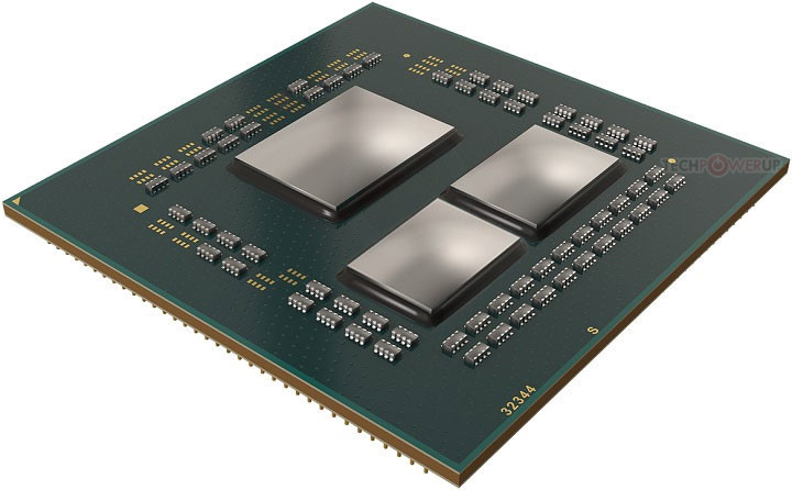
AMD's 3rd generation Ryzen (3000-series) processors will overcome a vast number of memory limitations faced by older Ryzen chips. With Zen 2, the company decided to separate the memory controller from the CPU cores into a separate chip, called "IO die". Our resident Ryzen memory guru Yuri "1usmus" Bubliy, author of DRAM Calculator for Ryzen, found technical info that confirms just how much progress AMD has been making.

The third generation Ryzen processors will be able to match their Intel counterparts when it comes to memory overclocking. In the Zen 2 BIOS, the memory frequency options go all the way up to "DDR4-5000", which is a huge increase over the first Ryzens. The DRAM clock is still linked to the Infinity Fabric (IF) clock domain, which means at DDR4-5000, Infinity Fabric would tick at 5000 MHz DDR, too. Since that rate is out of reach for IF, AMD has decided to add a new 1/2 divider mode for their on-chip bus. When enabled, it will run Infinity Fabric at half the DRAM actual clock (eg: 1250 MHz for DDR4-5000).

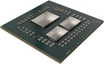
This could turn into an additional selling point for AMD X570 chipset motherboards, as they'll have a memory frequency headroom advantage over boards based on older chipsets as their BIOS will include not just the increased memory clock limit, but also the divider mode. Of course this doesn't mean that you can just magically overclock any memory kit to these 5 GHz speeds - it's probable that only the best of the best modules will be able to get close to these speeds.

1usmus also discovered that the platform adds a SoC OC mode and VDDG voltage control. We've heard from several sources that AMD invested heavily in improving memory compatibility, especially in the wake of Samsung discontinuing its B-die DRAM chips.
Add your own comment

112 Comments on AMD Ryzen 3000 "Zen 2" a Memory OC Beast, DDR4-5000 Possible

#76
Redwoodz
mat9v1/2 divider is kinda useless?
I mean, you get very fast memory and have to push it through a thin straw of halved IF to CPU cores. Sure if IF at 1250Mhz is significantly faster than memory at 5000 then it is not a big issue but if not - you loose that gained speed from increasing memory frequency. The more important thing when running IF at half speed would be timings. Whatever you gain from better timings in memory modules you loose much more in IF lagging behind - memory chip optimisation would gain us 10-20ns while IF running at half speed would loose us a 50ns easily? Consider that without any optimisations we get over 100ns for 2133 memory and corresponding 1066 IF speed and around 80 for 3200 memory and 1600 IF link - that is 20ns lag for 500Mhz of IF link speed. Sure increasing IF link speed would give us decreasingly smaller gains but still... going from 4000 memory with IF at 2000 to IF at 1000 would "kill the performance dead" ;)
It's good only for breaking speed records.

Now, if AMD would be to introduce 2x IF multiplier, that would enable use to lower delays introduced by slow IF link...
Consider somewhat slow memory at 3000 that results in IF running at 1500 and apply 2x to that to get IF running at 3000? IF link with delays on the order of 25ns... and even with low quality memory running at 2133 or 2400 we would get IF running at 2133 and 2400. It would eliminate the problem with IF bus concurrency when communicating with memory controller and PCIEx (GPUs) that can happen in current scenarios. All that, if IF would be able to run at that speeds.... but considering that some memory kits are able to run 3733 on ZEN+ and that means 1866 for IF it is not really far from 2133...

One can dream of course.
More options are always better. Besides, if they can get BLK adjustments working as well it takes the limitations off because then you can run whatever IF speed you want.
Posted on Reply
#77
mat9v
londisteRAM speed through IF should not be a problem. What Ryzen so far benefits from with fast memory is the increased IF link speed between CCXs which should be slower no matter what memory timings or speed gets to be. Faster memory does provide its own benefits but this is separate and even comparatively slow IF link should be enough for RAM's purposes.
IF speed impacts all reads from and to memory just because it is between cores and memory. Games running on two CCXs only compound the problem but forcing them to run on only 4 cores from single CCX does not fix much if anything. It is those delayed reads and writes from/to memory that are the problem, not the link speed but delays introduced by IF link.
It is not like IF is so fast anyway, according to AMD it runs at 42GB/s at 1333Mhz (or 2666 memory clock) according to
fuse.wikichip.org/news/1064/isscc-2018-amds-zeppelin-multi-chip-routing-and-packaging/
and that is very close to what memory benchmarks show for memory alone clocked at 3000Mhz. And yet, IF must also handle inter-CCX communication and PCIEx access - all that is overloading it's capacity.
Running it at twice the speed would be very good for performance if not power budget and yes I suppose AMD was not able to do so with ZEN/ZEN+, but I had hoped for ZEN2 to make it so.
Posted on Reply
#78
Super XP
I read somewhere that Infinity Fabric will no longer be tied to the IMC. Because in order for the fabric to achieve a set bandwidth, it cannot be tied to the IMC. It's because of how ZEN2 is designed. By having a 14nm and 7nm chiplets. I'll see if I can find that preview then post it.
Posted on Reply
#79
The Stilt
This has to be the new low from TPU, or frankly one of the many in recent times.

Stating that "DDR-5000MHz is possible" simply based on the available bios options is silly and makes no favors to anyone, the least to AMD. The same way you could state that with the current generation Ryzen CPUs DDR-4133MHz is possible, or that on Intel Coffee Lake Refresh parts DDR-5500MHz is possible. In reality of course, most current generation Ryzen users still struggle reaching higher than 3466MHz and the same way the typical best case scenario for daily use on Intel platforms is roughly 4133MHz or less (mostly due to the DRAM PCB or MB PCB signaling limits).

Actually both current gen. Ryzens already support up to DDR-8466MHz by their Phy design, but lets no let the facts to get in the way of fabricating the "news".

As I said, reporting BS like this (and the majority of other Zen 2 related rumors) is not in anyones interests.

Matisse will no doubt bring good improvements in most areas (incl. memory speeds), but everyone should keep their expectations at sane levels regardless.

If w1zzard was dead, he'd be spinning in his grave... :(
Posted on Reply
#80
Super XP
The StiltThis has to be the new low from TPU, or frankly one of the many in recent times.

Stating that "DDR-5000MHz is possible" simply based on the available bios options is silly and makes no favors to anyone, the least to AMD. The same way you could state that with the current generation Ryzen CPUs DDR-4133MHz is possible, or that on Intel Coffee Lake Refresh parts DDR-5500MHz is possible. In reality of course, most current generation Ryzen users still struggle reaching higher than 3466MHz and the same way the typical best case scenario for daily use on Intel platforms is roughly 4133MHz or less (mostly due to the DRAM PCB or MB PCB signaling limits).

Actually both current gen. Ryzens already support up to DDR-8466MHz by their Phy design, but lets no let the facts to get in the way of fabricating the "news".

As I said, reporting BS like this (and the majority of other Zen 2 related rumors) is not in anyones interests.

Matisse will no doubt bring good improvements in most areas (incl. memory speeds), but everyone should keep their expectations at sane levels regardless.

If w1zzard was dead, he'd be spinning in his grave... :(
Well I agree to a certain extent. Seems TPU isn't the only site reporting on this particular news.

As I said before, in my previous post. It seems Infinity Fabric will require at least 100 GB/s Bandwidth bidirectional in order to have enough to feed the 7nm Chiplets and the larger 14nm IO die.

I was under the impression the limiting factor for Infinity Fabric was the fact it was tied to the IMC. I still believe that's the case and the issue overall.
Posted on Reply
#81
bug
Super XPWell I agree to a certain extent. Seems TPU isn't the only site reporting on this particular news.
Well, the news is DDR4-5000 was found somewhere in Zen2's UEFI. TPU ups the ante and reports DDR4-5000 is possible with Zen2. There's a "slight" disconnect there. I don't have much of an issue with that, because I can understand what's being said, but you know many people don't read past the headlines.
Posted on Reply
#82
The Stilt
Super XPWell I agree to a certain extent. Seems TPU isn't the only site reporting on this particular news.

As I said before, in my previous post. It seems Infinity Fabric will require at least 100 GB/s Bandwidth bidirectional in order to have enough to feed the 7nm Chiplets and the larger 14nm IO die.

I was under the impression the limiting factor for Infinity Fabric was the fact it was tied to the IMC. I still believe that's the case and the issue overall.
SDF ("IF") is still tied to the MEMCLK, but this time around there is a Pll in between, which allows other than 1:1 frequency relation.

The intention is not to provide higher SDF bandwidth through higher frequency, but to allow higher MEMCLK frequencies (at a cost) to provide sufficient memory bandwidth.
Zen 2 is a wide core, and even Intel Xeons with 256-bit memory interface (QCH) become bandwidth starved in certain 256-bit workloads (not to mention 512-bit ones, hence SKL-SP uses 384-bit HCH memory config).
Posted on Reply
#83
R0H1T
mat9vAnd yet, IF must also handle inter-CCX communication and PCIEx access - all that is overloading it's capacity.
We don't know the layout of zen2 die, it could well be 8 cores per CCX or they might have changed the entire layout radically.
Posted on Reply
#84
Redwoodz
The StiltThis has to be the new low from TPU, or frankly one of the many in recent times.

Stating that "DDR-5000MHz is possible" simply based on the available bios options is silly and makes no favors to anyone, the least to AMD. The same way you could state that with the current generation Ryzen CPUs DDR-4133MHz is possible, or that on Intel Coffee Lake Refresh parts DDR-5500MHz is possible. In reality of course, most current generation Ryzen users still struggle reaching higher than 3466MHz and the same way the typical best case scenario for daily use on Intel platforms is roughly 4133MHz or less (mostly due to the DRAM PCB or MB PCB signaling limits).

Actually both current gen. Ryzens already support up to DDR-8466MHz by their Phy design, but lets no let the facts to get in the way of fabricating the "news".

As I said, reporting BS like this (and the majority of other Zen 2 related rumors) is not in anyones interests.

Matisse will no doubt bring good improvements in most areas (incl. memory speeds), but everyone should keep their expectations at sane levels regardless.

If w1zzard was dead, he'd be spinning in his grave... :(
bugWell, the news is DDR4-5000 was found somewhere in Zen2's UEFI. TPU ups the ante and reports DDR4-5000 is possible with Zen2. There's a "slight" disconnect there. I don't have much of an issue with that, because I can understand what's being said, but you know many people don't read past the headlines.
Yes it is an overstatement, thread author would have been better off showing that the new Biostar X570 has supports DDR4 4000+OC right on it's box.......meaning it HAS to be able to reach those speeds in at least some cases or they will be sued.
Posted on Reply
#85
Super XP
Well one goal for AMD should be to rectify the Infinity Fabric Latency hit. Hopefully they fixed this with the upcoming ZEN2 design.
Posted on Reply
#86
MikeMurphy
ImsochoboYes and no, a few times memory bandwidth is important.
But take a i9 14 core, remove two sticks and do dual channel, surprise!
Doesn't affect it that much at all!

Zens major limitation is latency more than bandwidth.
But surprise! Frequency decreases latency.

So yeah, to some extent bandwidth but I feel the latency is really what they are after.
Low latency memory doesn't solve the problem of 32 threads competing for access to that memory. Bandwidth does.
Posted on Reply
#87
bug
Super XPWell one goal for AMD should be to rectify the Infinity Fabric Latency hit. Hopefully they fixed this with the upcoming ZEN2 design.
We'll know soon enough.
MikeMurphyLow latency memory doesn't solve the problem of 32 threads competing for access to that memory. Bandwidth does.
In theory, low-latency is better when you need to access bits of memory frequently. But we already have 3 layers of cache take care of that. So yeah, bandwidth with be #1 on my watchlist too.
Posted on Reply
#88
londiste
R0H1TWe don't know the layout of zen2 die, it could well be 8 cores per CCX or they might have changed the entire layout radically.
Didn't @1usmus dig out the confirmation of 4-core CCX from BIOS images?
Posted on Reply
#91
londiste
Super XPBy utilizing 7nm Chiplets AMD can custom build CCXs with potentially 2 or 3 or 4 or 6 or 8 cores etc.
Well that is what I read once that's it's possible all by moving everything on that 14nm I/O and keeping the CPU chipsets separate. Who knows really.
CPU Complex (CCX) is the primary arhitectural multicore building block of Zen architectures. CCX size has nothing to do with I/O core, chiplets or 7nm.
Posted on Reply
#92
Super XP
londisteCPU Complex (CCX) is the primary arhitectural multicore building block of Zen architectures. CCX size has nothing to do with I/O core, chiplets or 7nm.
Perhaps I didn't make my comment clear enough. That 14nm IO can remain the same, keeping costs down all while allowing more customization with the 7nm chiplets.
Quote:
Of particular note, the chip incorporates a new-to-AMD chiplet based design approach, using separate I/O and CPU dies to simplify manufacturing and allow for easier chip customization.
www.anandtech.com/show/14286/amd-7nm-navi-gpu-and-rome-cpu-to-launch-in-q3
Posted on Reply
#93
londiste
Super XPPerhaps I didn't make my comment clear enough. That 14nm IO can remain the same, keeping costs down all while allowing more customization with the 7nm chiplets.
You are not using correct terminology then.

CCX is - as its name says - a core complex. In Zen it contains 4 cores and L3 cache (when looking at it on a high level). In a Zen/Zen+ chip die there are two such CCXs connected to Scalable Data Fabric (SDF) that we can characterize as IF hub where everything in the CPU connects to - CCXs, memory controllers, IO Hub. There is only one CCX configuration, while individual cores can be disabled in it there will not be multiple CCX configurations in the same generation. There are good reasons for expecting CCXs to remain at 4 cores in Zen 2.

Cores per die and cores per package are decidedly different from architectural features.

Amount of cores in Zen 2 CCX that we do not know is important because cores inside CCX can very quickly communicate with each other but communication with cores in a different CCX (even when it is on the same die) takes longer as it goes through IF connections.
Posted on Reply
#94
Super XP
Thanks for the explanation, I'm already aware of the inner workings of the CCX.

It's just that I read somewhere in a previous article (Pre ZEN+ release), where the author speculated that one possible reason for utilizing this ZEN2 design approach was to potentially benefit from customizable 7nm Chiplets.

Anyhow, your explanation is clarity enough. Thank You,
Posted on Reply
#95
londiste
Super XPIt's just that I read somewhere in a previous article (Pre ZEN+ release), where the author speculated that one possible reason for utilizing this ZEN2 design approach was to potentially benefit from customizable 7nm Chiplets.
Chiplet design benefits from higher yields due to smaller individual dies. This makes the design much cheaper than monolithic die with the same core count. This is practically the only benefit but it is a big one.

There are some negatives as well. IF links between dies is slightly slower in its current form and does use more power. Whether chiplet design adds complexity to the package is not sure yet but it is likely. With memory controller in the I/O die, memory is inevitably further away from the CPU cores, increasing latency. How much and how AMD has mitigated that - we will see soon.

Customizable chiplets can be a huge boon for custom market - consoles primarily. Maybe (a big maybe) for laptops. On desktop as we know it, customizable chiplets in terms of adding a GPU for an APU does not look like too good of a solution. With I/O Die, memory is far away and GPU is very dependent on memory (usually more bandwidth than latency but still). AM4 does not have enough space or pins to add HBM or some direct connected RAM. TR4/SM3 are unlikely candidates for integrated GPU.

There are a lot of thoughts being shared about stacked dies but with current CPU parts (including 7nm), power density will be a huge problem.
Posted on Reply
#96
Redwoodz
londisteChiplet design benefits from higher yields due to smaller individual dies. This makes the design much cheaper than monolithic die with the same core count. This is practically the only benefit but it is a big one.

There are some negatives as well. IF links between dies is slightly slower in its current form and does use more power. Whether chiplet design adds complexity to the package is not sure yet but it is likely. With memory controller in the I/O die, memory is inevitably further away from the CPU cores, increasing latency. How much and how AMD has mitigated that - we will see soon.

Customizable chiplets can be a huge boon for custom market - consoles primarily. Maybe (a big maybe) for laptops. On desktop as we know it, customizable chiplets in terms of adding a GPU for an APU does not look like too good of a solution. With I/O Die, memory is far away and GPU is very dependent on memory (usually more bandwidth than latency but still). AM4 does not have enough space or pins to add HBM or some direct connected RAM. TR4/SM3 are unlikely candidates for integrated GPU.

There are a lot of thoughts being shared about stacked dies but with current CPU parts (including 7nm), power density will be a huge problem.
Yes but I/O die on a cool, mature 14nm could be clocked high enough to mitigate that latency.
Posted on Reply
#97
londiste
RedwoodzYes but I/O die on a cool, mature 14nm could be clocked high enough to mitigate that latency.
What would be clocked high enough? Memory controller is tied to memory speed but the resulting bandwidth needs to fit through IF. IF has two endpoints, the other one is in the CPU cores' chiplet. Their best bet is probably making IF wider.
Posted on Reply
#98
Midland Dog
londisteLess memory modules is better than more memory modules. Go for 2x16GB instead of 4x8GB (assuming same speeds etc).
asssuming your cpu has a 128bit imc yeah, anything more than bandwidth goes up exponentially by using all channels
Posted on Reply
#99
Gasaraki
Motherboard BIOS options doesn't mean it's work at that speed.
Posted on Reply
#100
Redwoodz
londisteWhat would be clocked high enough? Memory controller is tied to memory speed but the resulting bandwidth needs to fit through IF. IF has two endpoints, the other one is in the CPU cores' chiplet. Their best bet is probably making IF wider.
Supposedly not tied strictly 1:1 now. What I meant is everything on Zen+ is 12nm. With I/O die on package @ 14nm they do not have to be tied @ 1:1 ratio.
londisteWhat would be clocked high enough? Memory controller is tied to memory speed but the resulting bandwidth needs to fit through IF. IF has two endpoints, the other one is in the CPU cores' chiplet. Their best bet is probably making IF wider.
What I mean is Zen+ is all 12nm.... 14nm I/O die on package is not tied @ 1:1 ratio.
Posted on Reply
Add your own comment
Oct 19th, 2024 03:54 EDT change timezone

New Forum Posts

Popular Reviews

Controversial News Posts