Thursday, May 23rd 2019

AMD X570 Unofficial Platform Diagram Revealed, Chipset Puts out PCIe Gen 4
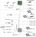
AMD X570 is the company's first in-house design socket AM4 motherboard chipset, with the X370 and X470 chipsets being originally designed by ASMedia. With the X570, AMD hopes to leverage new PCI-Express gen 4.0 connectivity of its Ryzen 3000 Zen2 "Matisse" processors. The desktop platform that combines a Ryzen 3000 series processor with X570 chipset is codenamed "Valhalla." A rough platform diagram like what you'd find in motherboard manuals surfaced on ChipHell, confirming several features. To maintain pin-compatibility with older generations of Ryzen processors, Ryzen 3000 has the same exact connectivity from the SoC except two key differences.
On the AM4 "Valhalla" platform, the SoC puts out a total of 28 PCI-Express gen 4.0 lanes. 16 of these are allocated to PEG (PCI-Express graphics), configurable through external switches and redrivers either as single x16, or two x8 slots. Besides 16 PEG lanes, 4 lanes are allocated to one M.2 NVMe slot. The remaining 4 lanes serve as the chipset bus. With X570 being rumored to support gen 4.0 at least upstream, the chipset bus bandwidth is expected to double to 64 Gbps. Since it's an SoC, the socket is also wired to LPCIO (SuperIO controller). The processor's integrated southbridge puts out two SATA 6 Gbps ports, one of which is switchable to the first M.2 slot; and four 5 Gbps USB 3.x ports. It also has an "Azalia" HD audio bus, so the motherboard's audio solution is directly wired to the SoC. Things get very interesting with the connectivity put out by the X570 chipset.Update May 21st: There is also information on the X570 chipset's TDP.
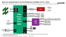
Update May 23rd: HKEPC posted what looks like an official AMD slide with a nicer-looking platform map. It confirms that AMD is going full-tilt with PCIe gen 4, both as chipset bus, and as downstream PCIe connectivity.
AMD X570 overcomes the greatest shortcoming of the previous-generation X470 "Promontory" chipset - downstream PCIe connectivity. The X570 chipset appears to put out 16 downstream PCI-Express gen 4.0 lanes. Two of these are allocated to two M.2 slots with x4 wiring, each, and the rest as x1 links. From these links, three are put out as x1 slots, one lane drives an ASMedia ASM1143 controller (takes in one gen 3.0 x1 and puts out two 10 Gbps USB 3.x gen 2 ports); one lane driving the board's onboard 1 GbE controller (choices include Killer E2500 or Intel i211-AT or even Realtek 2.5G); and one lane towards an 802.11ax WLAN card such as the Intel "Cyclone Peak." Other southbridge connectivity includes a 6-port SATA 6 Gbps RAID controller, four 5 Gbps USB 3.x gen 1 ports, and four USB 2.0/1.1 ports.
Update May 21st: The source also mentions the TDP of the AMD X570 chipset to be at least 15 Watts, a 3-fold increase over the X470 with its 5W TDP. This explains why every X570-based motherboard picture leak we've seen thus far shows a fan-heatsink over the chipset.
Sources:
ChipHell Forums, HKEPC
On the AM4 "Valhalla" platform, the SoC puts out a total of 28 PCI-Express gen 4.0 lanes. 16 of these are allocated to PEG (PCI-Express graphics), configurable through external switches and redrivers either as single x16, or two x8 slots. Besides 16 PEG lanes, 4 lanes are allocated to one M.2 NVMe slot. The remaining 4 lanes serve as the chipset bus. With X570 being rumored to support gen 4.0 at least upstream, the chipset bus bandwidth is expected to double to 64 Gbps. Since it's an SoC, the socket is also wired to LPCIO (SuperIO controller). The processor's integrated southbridge puts out two SATA 6 Gbps ports, one of which is switchable to the first M.2 slot; and four 5 Gbps USB 3.x ports. It also has an "Azalia" HD audio bus, so the motherboard's audio solution is directly wired to the SoC. Things get very interesting with the connectivity put out by the X570 chipset.Update May 21st: There is also information on the X570 chipset's TDP.
Update May 23rd: HKEPC posted what looks like an official AMD slide with a nicer-looking platform map. It confirms that AMD is going full-tilt with PCIe gen 4, both as chipset bus, and as downstream PCIe connectivity.
AMD X570 overcomes the greatest shortcoming of the previous-generation X470 "Promontory" chipset - downstream PCIe connectivity. The X570 chipset appears to put out 16 downstream PCI-Express gen 4.0 lanes. Two of these are allocated to two M.2 slots with x4 wiring, each, and the rest as x1 links. From these links, three are put out as x1 slots, one lane drives an ASMedia ASM1143 controller (takes in one gen 3.0 x1 and puts out two 10 Gbps USB 3.x gen 2 ports); one lane driving the board's onboard 1 GbE controller (choices include Killer E2500 or Intel i211-AT or even Realtek 2.5G); and one lane towards an 802.11ax WLAN card such as the Intel "Cyclone Peak." Other southbridge connectivity includes a 6-port SATA 6 Gbps RAID controller, four 5 Gbps USB 3.x gen 1 ports, and four USB 2.0/1.1 ports.
Update May 21st: The source also mentions the TDP of the AMD X570 chipset to be at least 15 Watts, a 3-fold increase over the X470 with its 5W TDP. This explains why every X570-based motherboard picture leak we've seen thus far shows a fan-heatsink over the chipset.


75 Comments on AMD X570 Unofficial Platform Diagram Revealed, Chipset Puts out PCIe Gen 4
Either way, socket information for AM4 and especially FP5 are somewhat hard to find, compared to their Intel counterparts.
3x PCIe x1 = 3 lanes
1x ASM1142 = 1 lane
1x E2500 = 1 lane
1x Wi-Fi = 1 lane
1x x4 slot = 4 lanes
That's 14...
A motherboard doesn't have to use all lanes...
As for speeds, I guess the unknown board maker also put 16GT/s between the CPU and chipset, which is also wrong so...
I also don't rely on TPUs information, but I guess you haven't read any of my other posts so...
Note that the source of the above diagram is a motherboard manufacture, so they've wired up the chipset the way they want.
I can guarantee that AMD wouldn't use Killer NICs for their own chipset diagrams.
I am looking to build a server build based on Zen 2 and an X570 motherboard and i was hoping Asrock would stick to having x8 SATA ports on their Taichi boards
Me, I just wonder if a more mainstream chipset will do away with multi-GPU support (which is waning anyway) and instead offer enough lanes to connect 3-4 NVMe drives directly to the CPU. Cause that will add more smoothness to the platform than a second GPU.
It would also be quite easy to just add a PCIe card with additional SATA ports if that's your only hangup.
Not without a switch...
a shame but ain't gonna complain about a platform that isn't even tested.
It's kind of how it has to work. Obviously with PCIe, we haven't had to change the physical interface for a few generations, so it has been a lot easier than in the past to transition to a new, faster version. Pointless is a very strong word in this case and you also seem to have missed the fact that there will be PCIe 4.0 NVMe SSDs coming out soon, which will reap benefits from the faster interface. How useful the extra speed will be to most people is a different matter. Also, as I mentioned elsewhere, this will allow for a single PCIe lane on 10Gbps Ethernet cards which might make them more affordable and more common.