Thursday, May 23rd 2019

AMD X570 Unofficial Platform Diagram Revealed, Chipset Puts out PCIe Gen 4
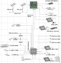
AMD X570 is the company's first in-house design socket AM4 motherboard chipset, with the X370 and X470 chipsets being originally designed by ASMedia. With the X570, AMD hopes to leverage new PCI-Express gen 4.0 connectivity of its Ryzen 3000 Zen2 "Matisse" processors. The desktop platform that combines a Ryzen 3000 series processor with X570 chipset is codenamed "Valhalla." A rough platform diagram like what you'd find in motherboard manuals surfaced on ChipHell, confirming several features. To maintain pin-compatibility with older generations of Ryzen processors, Ryzen 3000 has the same exact connectivity from the SoC except two key differences.
On the AM4 "Valhalla" platform, the SoC puts out a total of 28 PCI-Express gen 4.0 lanes. 16 of these are allocated to PEG (PCI-Express graphics), configurable through external switches and redrivers either as single x16, or two x8 slots. Besides 16 PEG lanes, 4 lanes are allocated to one M.2 NVMe slot. The remaining 4 lanes serve as the chipset bus. With X570 being rumored to support gen 4.0 at least upstream, the chipset bus bandwidth is expected to double to 64 Gbps. Since it's an SoC, the socket is also wired to LPCIO (SuperIO controller). The processor's integrated southbridge puts out two SATA 6 Gbps ports, one of which is switchable to the first M.2 slot; and four 5 Gbps USB 3.x ports. It also has an "Azalia" HD audio bus, so the motherboard's audio solution is directly wired to the SoC. Things get very interesting with the connectivity put out by the X570 chipset.Update May 21st: There is also information on the X570 chipset's TDP.
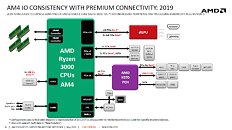
Update May 23rd: HKEPC posted what looks like an official AMD slide with a nicer-looking platform map. It confirms that AMD is going full-tilt with PCIe gen 4, both as chipset bus, and as downstream PCIe connectivity.
AMD X570 overcomes the greatest shortcoming of the previous-generation X470 "Promontory" chipset - downstream PCIe connectivity. The X570 chipset appears to put out 16 downstream PCI-Express gen 4.0 lanes. Two of these are allocated to two M.2 slots with x4 wiring, each, and the rest as x1 links. From these links, three are put out as x1 slots, one lane drives an ASMedia ASM1143 controller (takes in one gen 3.0 x1 and puts out two 10 Gbps USB 3.x gen 2 ports); one lane driving the board's onboard 1 GbE controller (choices include Killer E2500 or Intel i211-AT or even Realtek 2.5G); and one lane towards an 802.11ax WLAN card such as the Intel "Cyclone Peak." Other southbridge connectivity includes a 6-port SATA 6 Gbps RAID controller, four 5 Gbps USB 3.x gen 1 ports, and four USB 2.0/1.1 ports.
Update May 21st: The source also mentions the TDP of the AMD X570 chipset to be at least 15 Watts, a 3-fold increase over the X470 with its 5W TDP. This explains why every X570-based motherboard picture leak we've seen thus far shows a fan-heatsink over the chipset.
Sources:
ChipHell Forums, HKEPC
On the AM4 "Valhalla" platform, the SoC puts out a total of 28 PCI-Express gen 4.0 lanes. 16 of these are allocated to PEG (PCI-Express graphics), configurable through external switches and redrivers either as single x16, or two x8 slots. Besides 16 PEG lanes, 4 lanes are allocated to one M.2 NVMe slot. The remaining 4 lanes serve as the chipset bus. With X570 being rumored to support gen 4.0 at least upstream, the chipset bus bandwidth is expected to double to 64 Gbps. Since it's an SoC, the socket is also wired to LPCIO (SuperIO controller). The processor's integrated southbridge puts out two SATA 6 Gbps ports, one of which is switchable to the first M.2 slot; and four 5 Gbps USB 3.x ports. It also has an "Azalia" HD audio bus, so the motherboard's audio solution is directly wired to the SoC. Things get very interesting with the connectivity put out by the X570 chipset.Update May 21st: There is also information on the X570 chipset's TDP.
Update May 23rd: HKEPC posted what looks like an official AMD slide with a nicer-looking platform map. It confirms that AMD is going full-tilt with PCIe gen 4, both as chipset bus, and as downstream PCIe connectivity.
AMD X570 overcomes the greatest shortcoming of the previous-generation X470 "Promontory" chipset - downstream PCIe connectivity. The X570 chipset appears to put out 16 downstream PCI-Express gen 4.0 lanes. Two of these are allocated to two M.2 slots with x4 wiring, each, and the rest as x1 links. From these links, three are put out as x1 slots, one lane drives an ASMedia ASM1143 controller (takes in one gen 3.0 x1 and puts out two 10 Gbps USB 3.x gen 2 ports); one lane driving the board's onboard 1 GbE controller (choices include Killer E2500 or Intel i211-AT or even Realtek 2.5G); and one lane towards an 802.11ax WLAN card such as the Intel "Cyclone Peak." Other southbridge connectivity includes a 6-port SATA 6 Gbps RAID controller, four 5 Gbps USB 3.x gen 1 ports, and four USB 2.0/1.1 ports.
Update May 21st: The source also mentions the TDP of the AMD X570 chipset to be at least 15 Watts, a 3-fold increase over the X470 with its 5W TDP. This explains why every X570-based motherboard picture leak we've seen thus far shows a fan-heatsink over the chipset.


75 Comments on AMD X570 Unofficial Platform Diagram Revealed, Chipset Puts out PCIe Gen 4
All NVMe ports on this diagram (be it from CPU or chipset) are either PCIEx 3.0 x4 or PCIEx 4.0 x2 - that's what 32Gbps stands for.
Should we understand that Ryzen 3xxx CPUs will not have USB Gen2 support built-in and will depend on chipset to provide one? Why?
Why use ASM1143 to provide only one USB Gen2 port?
This whole thing makes no sense to me.
It seems like a lot of things are labelled wrong as well. Maybe someone forgot to update the numbers?
The chipset to CPU link is also too narrow in terms of GT/s.
No, the two ports below the ASM1143 are Gen 2.
No logic as far as I can tell.
Again, poorly designed board, it happens...
As I pointed out, this is not really representative of the X570 chipset based on what I know.
AM4 platform has two southbridges, one on the CPU silicon, one on the motherboard. The one on the CPU silicon talks to the K17 iNB over 4 PCIe lanes that are abstract. On a Threadripper or EPYC, the internal SB is disabled on all but one of the "Zeppelin" dies on the MCM. So those lanes are freed up.
The internal SB puts out SATA6G (two ports), USB3, LPCIO (Legacy/ISA), and HD Audio buses. The external SB augments additional SATA, USB, and downstream PCIe for things such as WLAN, GbE-PHY, USB3.1, etc.
I mean its just 15W TDP, surely it is possible, right?
Yes, it's possible.
What I speculated is for MB vendors to implement hybrid fan curve, to not spin until necessary, which should be most of the time.
What are these expensive cables you are talking about? an SFF+ to SFF+ cable (~€50) works out a lot cheaper than buying two copper NICs for example too.
So just because 15 watts isn't a lot, it can easily become a lot if you have no airflow. Just check out literally every fanless laptop that gets placed under load.
+ Maybe first PCI-E and M2 but no devices will use it, gpu's hardly stress 16x 3.0.. mostly 8x is enough.
In all seriousness, though: PCIe 5.0 is yet to be standardized, and given historical time spans from standardization to consumer hardware, we won't see that until late 2021 at the very earliest - and likely later than that given that it's heavily focused on server-specific functionality. DDR5 will likely arrive with AM5(?) and whatever consumer socket Intel launches in 2020-21. Intel tends to prioritize new RAM for HEDT and server, though, so we might have to wait longer than that. And where, exactly, is the harm in moving to PCIe 4.0 even if 5.0 were to arrive in just a few years? Someone has to start the push for faster interfaces on devices, and device manufacturers aren't going to invest in PCIe 4.0 controllers etc. if there are no PCs that support them. And given PCIe backwards compatibility, when 5.0 arrives this will mean that there's a decent selection of 4.0 devices on the market for those boards, rather than having to stick with 3.0 devices until 5.0 reaches GPUs, SSDs and the like. This is a win-win scenario, stop complaining....which is exactly what PCIe 4.0 allows for. How? By doubling bandwidth per lane. A PCIe 4.0 x2 SSD can match the performance of a PCIe 3.0 x4 SSD, meaning that you can run two fast SSDs off the same number of lanes as one previously. A single 4.0 lane is enough for a 10GbE NIC, where you previously needed two lanes. And so on and so forth. GPUs won't need more than x8 PCIe 4.0 for the foreseeable future (and in reality hardly more than x4 for most GPUs), so splitting off lanes for storage or other controllers is less of an issue. Sure, performance (or the advantage of splitting lanes) is lost if using PCIe 3.0 devices, but there is flexibility to be had - for example a motherboard might have two m.2 slots where they share the latter two lanes (switchable in BIOS, ideally) so that you can run either two ~3.5GB/s SSDs or one faster than that. Motherboard trace routing will also become less complex if the thinking shifts this way, leading to potentially cheaper motherboards or more features at lower price points.Not if the fans only run when needed - if so, it's arguably smart design, not lazy. Still, I would entirely welcome a return to functional heatsinks on motherboards. The EVGA x299 Dark sets a good precedent.
Technically external USB controllers shouldn't be needed, as all the USB 3 ports are 3.1 G2 and the chipset should support eight of them.
It really comes down to what the board makers do with the available lanes, as AMD has added what seems to be more than sufficient lanes imho.
I don't think eight of them has to be used for M.2 devices either (not counting the additional four from the CPU).
If anyone needs more than this, there is of course Threadripper and with luck an X599 or the like in due course.
On AM4 it only 24 lanes are activate for maybe compitability for reason with APU.
But on for Embedded server part all 32 Lanes are active.
www.amd.com/en/products/specifications/embedded/8161
@IceShroom Isn't it called "Zeppelin" like the air-ship?
I presume all that goes away with the CPU chiplet and moves to the I/O die. What exactly they have in there has kind of yet to be revealed fully.