Wednesday, October 28th 2020

AMD Announces the Radeon RX 6000 Series: Performance that Restores Competitiveness

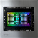
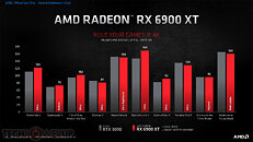
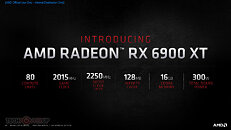
AMD (NASDAQ: AMD) today unveiled the AMD Radeon RX 6000 Series graphics cards, delivering powerhouse performance, incredibly life-like visuals, and must-have features that set a new standard for enthusiast-class PC gaming experiences. Representing the forefront of extreme engineering and design, the highly anticipated AMD Radeon RX 6000 Series includes the AMD Radeon RX 6800 and Radeon RX 6800 XT graphics cards, as well as the new flagship Radeon RX 6900 XT - the fastest AMD gaming graphics card ever developed.

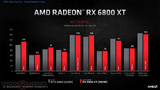
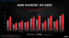
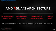
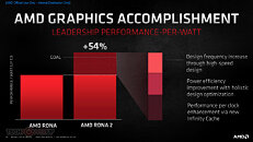
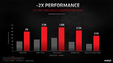
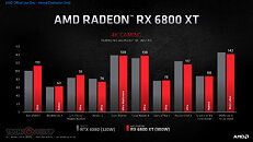
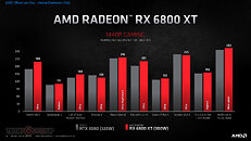
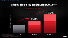
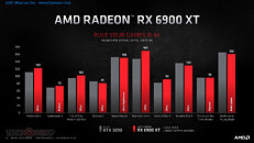
AMD Radeon RX 6000 Series graphics cards are built upon groundbreaking AMD RDNA 2 gaming architecture, a new foundation for next-generation consoles, PCs, laptops and mobile devices, designed to deliver the optimal combination of performance and power efficiency. AMD RDNA 2 gaming architecture provides up to 2X higher performance in select titles with the AMD Radeon RX 6900 XT graphics card compared to the AMD Radeon RX 5700 XT graphics card built on AMD RDNA architecture, and up to 54 percent more performance-per-watt when comparing the AMD Radeon RX 6800 XT graphics card to the AMD Radeon RX 5700 XT graphics card using the same 7 nm process technology.
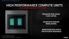
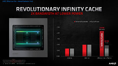
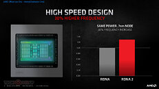
AMD RDNA 2 offers a number of innovations, including applying advanced power saving techniques to high-performance compute units to improve energy efficiency by up to 30 percent per cycle per compute unit, and leveraging high-speed design methodologies to provide up to a 30 percent frequency boost at the same power level. It also includes new AMD Infinity Cache technology that offers up to 2.4X greater bandwidth-per-watt compared to GDDR6-only AMD RDNA -based architectural designs.

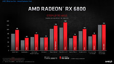
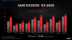
"Today's announcement is the culmination of years of R&D focused on bringing the best of AMD Radeon graphics to the enthusiast and ultra-enthusiast gaming markets, and represents a major evolution in PC gaming," said Scott Herkelman, corporate vice president and general manager, Graphics Business Unit at AMD. "The new AMD Radeon RX 6800, RX 6800 XT and RX 6900 XT graphics cards deliver world class 4K and 1440p performance in major AAA titles, new levels of immersion with breathtaking life-like visuals, and must-have features that provide the ultimate gaming experiences. I can't wait for gamers to get these incredible new graphics cards in their hands."

Powerhouse Performance, Vivid Visuals & Incredible Gaming Experiences
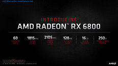
AMD Radeon RX 6000 Series graphics cards support high-bandwidth PCIe 4.0 technology and feature 16 GB of GDDR6 memory to power the most demanding 4K workloads today and in the future. Key features and capabilities include:

Powerhouse Performance
  • AMD Infinity Cache - A high-performance, last-level data cache suitable for 4K and 1440p gaming with the highest level of detail enabled. 128 MB of on-die cache dramatically reduces latency and power consumption, delivering higher overall gaming performance than traditional architectural designs.
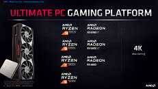
  • AMD Smart Access Memory - An exclusive feature of systems with AMD Ryzen 5000 Series processors, AMD B550 and X570 motherboards and Radeon RX 6000 Series graphics cards. It gives AMD Ryzen processors greater access to the high-speed GDDR6 graphics memory, accelerating CPU processing and providing up to a 13-percent performance increase on a AMD Radeon RX 6800 XT graphics card in Forza Horizon 4 at 4K when combined with the new Rage Mode one-click overclocking setting.9,10
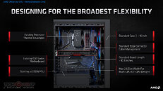
  • Built for Standard Chassis - With a length of 267 mm and 2x8 standard 8-pin power connectors, and designed to operate with existing enthusiast-class 650 W-750 W power supplies, gamers can easily upgrade their existing large to small form factor PCs without additional cost.
True to Life, High-Fidelity Visuals
  • DirectX 12 Ultimate Support - Provides a powerful blend of raytracing, compute, and rasterized effects, such as DirectX Raytracing (DXR) and Variable Rate Shading, to elevate games to a new level of realism.
  • DirectX Raytracing (DXR) - Adding a high performance, fixed-function Ray Accelerator engine to each compute unit, AMD RDNA 2-based graphics cards are optimized to deliver real-time lighting, shadow and reflection realism with DXR. When paired with AMD FidelityFX, which enables hybrid rendering, developers can combine rasterized and ray-traced effects to ensure an optimal combination of image quality and performance.
  • AMD FidelityFX - An open-source toolkit for game developers available on AMD GPUOpen. It features a collection of lighting, shadow and reflection effects that make it easier for developers to add high-quality post-process effects that make games look beautiful while offering the optimal balance of visual fidelity and performance.
  • Variable Rate Shading (VRS) - Dynamically reduces the shading rate for different areas of a frame that do not require a high level of visual detail, delivering higher levels of overall performance with little to no perceptible change in image quality.
Elevated Gaming Experience
  • Microsoft DirectStorage Support - Future support for the DirectStorage API enables lightning-fast load times and high-quality textures by eliminating storage API-related bottlenecks and limiting CPU involvement.
  • Radeon Software Performance Tuning Presets - Simple one-click presets in Radeon Software help gamers easily extract the most from their graphics card. The presets include the new Rage Mode stable over clocking setting that takes advantage of extra available headroom to deliver higher gaming performance.
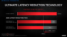
  • Radeon Anti-Lag - Significantly decreases input-to-display response times and offers a competitive edge in gameplay.
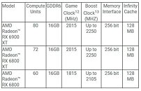
AMD Radeon RX 6000 Series Product Family
Robust Gaming Ecosystem and Partnerships
In the coming weeks, AMD will release a series of videos from its ISV partners showcasing the incredible gaming experiences enabled by AMD Radeon RX 6000 Series graphics cards in some of this year's most anticipated games. These videos can be viewed on the AMD website.
  • DIRT 5 - October 29
  • Godfall - November 2
  • World of Warcraft : Shadowlands - November 10
  • RiftBreaker - November 12
  • FarCry 6 - November 17
Pricing and Availability
  • AMD Radeon RX 6800 and Radeon RX 6800 XT graphics cards are expected to be available from global etailers/retailers and on AMD.com beginning November 18, 2020, for $579 USD SEP and $649 USD SEP, respectively. The AMD Radeon RX 6900 XT is expected to be available December 8, 2020, for $999 USD SEP.
  • AMD Radeon RX 6800 and RX 6800 XT graphics cards are also expected to be available from AMD board partners, including ASRock, ASUS, Gigabyte, MSI, PowerColor, SAPPHIRE and XFX, beginning in November 2020.
The complete AMD slide deck follows.
Add your own comment

394 Comments on AMD Announces the Radeon RX 6000 Series: Performance that Restores Competitiveness

#351
Valantar
lexluthermiesterPlus, they are focused on a new socket. The Ryzen 5000 series of CPU's is the last for socket AM4. The next will likely be AM5.
And they can't rush that out before PCIe 5.0 is at least technically viable (likely needs new on-board hardware to ensure signal integrity, which might not be available at consumer price levels for a while) and DDR5 has wide availability. Definitely good reasons to hold off AM5 for a while yet.

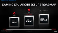
But using that as an argument that AMD will try to quicken their GPU development pace? Nah, sorry, not buying that. 16 months between RDNA 1 and RDNA 2. Now we're supposed to get RDNA 3 in < 14 months? And remember, a launch later in the year than this isn't happening no matter what. It's either pre holiday season or CES. Which makes that 12 months, not 14. I really don't see that as likely. I'll be more than happy to be proven wrong, but I'm definitely sticking to a more cautious approach here.
Posted on Reply
#352
R0H1T
Why do you think they'll just straight up go with PCIe 5.0 ? They most certainly can skip on that.

DDR5 is a given, PCIe 5.0 is not much of a necessity even on servers. Of course with Xilinx (acquisition) they might surprise us or something.
Posted on Reply
#353
Valantar
R0H1TWhy do you think they'll just straight up go with PCIe 5.0 ? They most certainly can skip on that.

DDR5 is a given, PCIe 5.0 is not much of a necessity even on servers. Of course with Xilinx they might surprise us or something.
I don't think it's necessary at all, but launching a new long-term platform ~a year before the availability of a I/O standard is generally a bad idea. Of course it's possible that they could launch AM5 with the promise of future PCIe 5.0 support (i.e. first-gen motherboards and CPUs will have 5.0, but will be compatible with next-gen CPUs and mobos that have 5.0 support, just at 4.0 speeds when mixed), but again, that's rather sloppy.
Posted on Reply
#354
dragontamer5788
Zach_01I think they are able to cut/disable CUs by 2. If you look RNDA1/2 full dies you will see 20 and 40 same rectangular respectively. Each one of these rectangular are 2CUs.
Note: CU is now a bit of a historical artifact. RDNA and RDNA 2 are organized into WGPs, or "Dual Compute Units" (because each WGP has the resources of 2x CUs of old). That's why there are 40 RDNA clusters, which count as 80 "CUs" (even though CUs don't really exist anymore).

CUs were in Vega, and are a decent unit to think about while programming the GPU. WGPs work really hard to "pretend" to work like 2x CUs for backwards compatibility purposes... but they're really just one unit now.

-----

As such: the proper term for those 40x clusters on your RDNA2 die shot is Workgroup Processor (WGP)... or "Dual-compute units" (if you want to make a comparison to Vega).
Posted on Reply
#355
BoboOOZ
ValantarBut using that as an argument that AMD will try to quicken their GPU development pace? Nah, sorry, not buying that. 16 months between RDNA 1 and RDNA 2. Now we're supposed to get RDNA 3 in < 14 months? And remember, a launch later in the year than this isn't happening no matter what. It's either pre holiday season or CES. Which makes that 12 months, not 14. I really don't see that as likely. I'll be more than happy to be proven wrong, but I'm definitely sticking to a more cautious approach here.
You forget that during these 16 months they effectively launched 3 architectures, RDNA2 + 2 custom APUs, with different architectures and features for consoles. Now the whole GPU design team is free to work on the new GPU generation.
Posted on Reply
#356
TheoneandonlyMrK
ValantarI don't think it's necessary at all, but launching a new long-term platform ~a year before the availability of a I/O standard is generally a bad idea. Of course it's possible that they could launch AM5 with the promise of future PCIe 5.0 support (i.e. first-gen motherboards and CPUs will have 5.0, but will be compatible with next-gen CPUs and mobos that have 5.0 support, just at 4.0 speeds when mixed), but again, that's rather sloppy.
They added pciex4 into zen later.
Posted on Reply
#357
Valantar
BoboOOZYou forget that during these 16 months they effectively launched 3 architectures, RDNA2 + 2 custom APUs, with different architectures and features for consoles. Now the whole GPU design team is free to work on the new GPU generation.
"The whole design team" is at least four separate design teams (two for Zen). It's not like all the Zen design engineers can just slot into a GPU design team without a significant retraining period. The semi-custom team is no doubt already working on 5nm refreshes for both console makers, but some of their engineers could have been moved to a field closer to their expertise, whether that's CPU, GPU, I/O, fabric, etc. Ryzen is under continuous development; one team just finished Zen 3, the other is hard at work with Zen 4, and no doubt the Zen 2 team is now ramping up development of Zen 5. There might be some minor shuffling, but nothing on the scale you are indicating.
theoneandonlymrkThey added pciex4 into zen later.
That's true. But that was quite a long time after AM4 launched, not a year or less.
Posted on Reply
#358
BoboOOZ
Valantar"The whole design team" is at least four separate design teams (two for Zen). It's not like all the Zen design engineers can just slot into a GPU design team without a significant retraining period. The semi-custom team is no doubt already working on 5nm refreshes for both console makers, but some of their engineers could have been moved to a field closer to their expertise, whether that's CPU, GPU, I/O, fabric, etc. Ryzen is under continuous development; one team just finished Zen 3, the other is hard at work with Zen 4, and no doubt the Zen 2 team is now ramping up development of Zen 5. There might be some minor shuffling, but nothing on the scale you are indicating.
I wonder where do you get the info on the console 5nm refreshes, do you have any source, or are you just guessing? Sony made it clear there will be no refreshes this generation, at least, and there is no leak or hint of that yet, if any of that will come, it will most probably be way later after RDNA3.
Posted on Reply
#359
TheoneandonlyMrK
BoboOOZI wonder where do you get the info on the console 5nm refreshes, do you have any source, or are you just guessing? Sony made it clear there will be no refreshes this generation, at least, and there is no leak or hint of that yet, if any of that will come, it will most probably be way later after RDNA3.
Doesn't mean they won't evolve what's out for a cheaper BOM, it's what they do.
Posted on Reply
#360
InVasMani
Zach_01My, absolutely based on (my) logic, estimation is that AMD will stay away from GDDR6X. Because they can get away with the new IC implementation. And second for the all kinds of expenses. GDDR6X is more expensive, draws almost X3 the power from “simple” GDDR6, and the memory controller need to be more complex too (=more expenses on die area and fab cost).

This I “heard” partially...
The three 6000 we’ve seen so far is based on the Navi21 right? 80CUs full die. They may have one more N21 with further less CUs, don’t know how many, probably 56 or even less active with 8GB(?) and probably same 256bit bus. But this isn’t coming soon I think because they may have to make inventory first (because of present good fab yields) and also see how things will go with nVidia.

Further down they have Navi22. Probably (?)40CUs full die with 192bit bus, (?)12GB, and clocks up to 2.5GHz, 160~200W, with who knows how much IC it will have. That will be better than 5700XT.
And also cutdown versions of N22 with 32~36CUs 8/10/12GB 160/192bit (for 5600/5700 replacements) and so on, but at this point is all on full speculations and things may change in future.

Also rumors for Navi23 with 24~32CUs but... it’s way too soon.

Navi21: 4K
Navi22: 1440p and ultrawide
Navi23: 1080p only
That does make sense on the GDDR6X situation on the cost, complexity, and power situation relative to GDDR6 and with the infinity cache being so effective. I'd like to think with 192-bit they'd have more than 40CU's considering the infinity cache. If it were 128-bit with 64MB infinity cache I could see something like 36CU even being quite reasonable. I think trying to aim higher than RNDA1 is in AMD's best interest for both longevity and margins or at least matching it at better efficiency and cost to produce.
ValantarYep, CUs are grouped two by two in ... gah, I can't remember what they call the groups. Anyhow, AMD can disable however many they like as long as it's a multiple of 2.
Looking at them I actually wouldn't expect them to cut that few realistically for a few reasons obviously SKU differentiation is one obvious reason, but the other is heat distribution balance. I'm not sure that's really ideal cutting 4CU's in total with slices of 2CU's diagonal from each other on opposite sides of the die itself kind of makes more sense. That said AMD has a lot of tech packed into their circuitry these days with precision boost and granular management over them that they probably cut only 2CU's if they felt inclined and not have to worry drastically about the heat management and hot spots becoming a real concerning aspect. If it were me I'd probably approach like I described trying to keep heat distribution most efficient when cutting the CU's down. The SKU differentiation is really the biggest concern I feel though I don't think they are going to slice these up 50 ways to kingdom come myself unless they were trying stirr up a bit of a bidding contract war between the AIB's for slightly better binned SKU's of die's in rather finely incremental differentiating ways. I suppose it could happen, but depends on added time and cost to sort thru all that.
Posted on Reply
#361
Valantar
BoboOOZI wonder where do you get the info on the console 5nm refreshes, do you have any source, or are you just guessing? Sony made it clear there will be no refreshes this generation, at least, and there is no leak or hint of that yet, if any of that will come, it will most probably be way later after RDNA3.
No source, but every single console generation since the PS1 has had some sort of refresh. I'm not talking about the new tier, mid-generation upgrades that we saw with the current generation. Refresh = same specs, new process, smaller, cheaper die with lower power draw. The PS1 had at least one slim version. The PS2 had at least 2. I don't think the OG Xbox had one, but the 360 had two, and the One had one (the S). The PS3 had at least a couple, and the PS4 had one (the Slim). Given that 5nm is already in volume production today, it stands to reason that it'll be cheap enough in 2-3 years that console makers will want to move to it. Even if the cost per die is the same due to the more advanced process, they'll save on the BOM through lower power draw = smaller PSU and heatsink.
InVasManiLooking at them I actually wouldn't expect them to cut that few realistically for a few reasons obviously SKU differentiation is one obvious reason, but the other is heat distribution balance. I'm not sure that's really ideal cutting 4CU's in total with slices of 2CU's diagonal from each other on opposite sides of the die itself kind of makes more sense. That said AMD has a lot of tech packed into their circuitry these days with precision boost and granular management over them that they probably cut only 2CU's if they felt inclined and not have to worry drastically about the heat management and hot spots becoming a real concerning aspect. If it were me I'd probably approach like I described trying to keep heat distribution most efficient when cutting the CU's down. The SKU differentiation is really the biggest concern I feel though I don't think they are going to slice these up 50 ways to kingdom come myself unless they were trying stirr up a bit of a bidding contract war between the AIB's for slightly better binned SKU's of die's in rather finely incremental differentiating ways. I suppose it could happen, but depends on added time and cost to sort thru all that.
I didn't say they would be cutting 2 off anything, I said they can cut any number as long as it's 2x something. I.e. 2, 4, 6, 8, 10, 12... Even numbered cuts only, in other words. Nor did I say anything about where they would be cut from - that is either decided by where on the die there are defects, or if there aren't any, whatever is convenient engineering-wise. To quote myself, this is my (very rough and entirely unsourced) guess for the Navi 2 lineup in terms of CUs:
Valantar80-72-60-(new die)-48-40-32-(new die)-28-24-20 sounds like a likely lineup to me, which gives us everything down to a 5500 non-XT, with the possibility of 5400/5300 SKUs with disabled memory, lower clocks, etc.
Posted on Reply
#364
InVasMani
ValantarI didn't say they would be cutting 2 off anything, I said they can cut any number as long as it's 2x something. I.e. 2, 4, 6, 8, 10, 12... Even numbered cuts only, in other words. Nor did I say anything about where they would be cut from - that is either decided by where on the die there are defects, or if there aren't any, whatever is convenient engineering-wise. To quote myself, this is my (very rough and entirely unsourced) guess for the Navi 2 lineup in terms of CUs:
I was injecting my thoughts on the 2CU situation or twin units whatever you wish to call them or abbreviate them. What I was saying is it's unlikely AMD would bother with a SKU that differentiates by as few as 2 of the CU's seems most probably it would be someplace between 6 to 12 between two different SKU's to me at this point. I do see AMD leaning toward cutting less CU's where possible though and charging a higher premium for better performance and CU count is probably greatly more important than the bandwidth with the current design it's needed to make full advantage of the bandwidth available. Much of what happens hinges on the infinity cache size and bus width in any future SKU's even outside VRAM that also change things a fair bit HBM2 with infinity cache for new SKU's with even more CU's is a real possible scenario to consider too even w/o changing the bus width that's tons of extra bandwidth and more CU's to go along with it and the HBM2 is more power friendly than the GDDR6 if I'm not mistaken along with occupying less space so a bigger chip is rather tangible though I don't know about the yields of that. That said they could do 3SKU's lower initially then try to build a bigger higher CU count chip with HBM2 in that order to maximize the yields situation because TSMC's node will continue to mature more over time. The cost factor would be the concern with HBM2, but it would be better power, bandwidth, and space savings.
FluffmeisterYeah not sure if it was posted but AMD up benchmarks with SAM enabled but no rage mode.

www.amd.com/en/gaming/graphics-gaming-benchmarks

Results chop and change a bit, but it gives an idea what to expect.
That's quite interesting once you drop from 4K to 1440p RNDA2 performance pulls ahead rapidly relative to Ampere. I'd really like to see AMD add 1080p results to this list of benchmarks. The infinity cache seems to really flex it's benefit the most at lower resolutions in perticular which makes sense given the limited amount of cache to work with and huge latency reduction and bandwidth increase it provides better mileage of it naturally. It's actually very much akin to the Intel situation at 1080p so long for eleague high refresh rate gaming. I presume these cards are going to sell like hot cakes to that crowd of users because these cards will scream along nicely at 1080p high refresh rate far as I'm seeing relative to the cost. It'll be interesting to see what happens with RTRT at different resolutions. That infinity cache seems really well effective at lower resolutions.
Posted on Reply
#365
Zach_01
InVasManiThat's quite interesting once you drop from 4K to 1440p RNDA2 performance pulls ahead rapidly relative to Ampere. I'd really like to see AMD add 1080p results to this list of benchmarks. The infinity cache seems to really flex it's benefit the most at lower resolutions in perticular which makes sense given the limited amount of cache to work with and huge latency reduction and bandwidth increase it provides better mileage of it naturally. It's actually very much akin to the Intel situation at 1080p so long for eleague high refresh rate gaming. I presume these cards are going to sell like hot cakes to that crowd of users because these cards will scream along nicely at 1080p high refresh rate far as I'm seeing relative to the cost.
If you think AMDs latest performance across resolutions relatively to Ampere seems that it doesn’t do well on the higher/highest.

It’s not really that RDNA2 architecture/IC doesn’t scale well on different resolutions. Or that it does better at lower ones. It’s the Ampere architecture that doesn’t scale well across resolutions.
And you can see that from benchmarks comparing Turing vs Ampere. Turing and RDNA2 have a more “normal” scaling across the 3 well known 1080p, 1440p and 4K.

Seeing benchmarks of Turing vs Ampere across the 3 res you can identify that as you going up Ampere is getting away from Turing to reach the avg relative perf gains of around 30% on 4K. But on 1080p that difference is “only” 20%.
It’s a matter of Ampere’s architecture.

Also, this relative comparison (we don’t actually have full benches between Turing and RDNA2) short of confirms that AMD’s IC with the high (effective) bandwidth is working well and delivers its promises as a real wide bus.
Posted on Reply
#366
Valantar
Zach_01If you think AMDs latest performance across resolutions relatively to Ampere seems that it doesn’t do well on the higher/highest.

It’s not really that RDNA2 architecture/IC doesn’t scale well on different resolutions. Or that it does better at lower ones. It’s the Ampere architecture that doesn’t scale well across resolutions.
And you can see that from benchmarks comparing Turing vs Ampere. Turing and RDNA2 have a more “normal” scaling across the 3 well known 1080p, 1440p and 4K.

Seeing benchmarks of Turing vs Ampere across the 3 res you can identify that as you going up Ampere is getting away from Turing to reach the avg relative perf gains of around 30% on 4K. But on 1080p that difference is “only” 20%.
It’s a matter of Ampere’s architecture.

Also, this relative comparison (we don’t actually have full benches between Turing and RDNA2) short of confirms that AMD’s IC with the high (effective) bandwidth is working well and delivers its promises as a real wide bus.
AFAIK that is mainly because it's only at 4k (and higher) that you can make any real use of the increased FP32 of Ampere, while at lower resolutions you're bottlenecked by other parts of the arch (which weren't doubled).
Posted on Reply
#367
InVasMani
I'll assume you're probably right about Ampere, but far as the resolution scaling is concerned for RDNA2 1080p will be better use of the bandwidth available than 4K more frames for the same amount of bandwidth assuming the CPU can keep pace and the GPU's CU's can keep all that bandwidth availability fed well enough. All I know is RDNA2 relative to Ampere the scaling on RDNA2 did noticeably better when the resolution scaled down from 4K to 1440p and I suspect that follows thru to 1080p as well because it wasn't like a anomaly from the looks of it at all it was across all the tests the gaps narrows or RNDA2 pulls ahead or pulled away even further. You might be right about Ampere, but the infinity cache could be playing a role on top of that much like a SSD with overprovisioning at a lower resolution you'll have more infinity cache overprovisioning to work with so to speak.
Posted on Reply
#368
Zach_01
I guess this “issue” will be cleared as benchmarks will go public with all architectures in them on all resolutions.
Posted on Reply
#369
InVasMani
I'm confusing myself trying to think about it now honestly. I get what you're saying about Ampere, but at the same time the infinity cache is drastically better on bandwidth and I/O. At lower resolution it could come into play more in terms of being readily obvious to the frame rate impact over a given time frame if the CPU/GPU's other requirements and needs can still lift their weight in accordance as well. I need to see a clearer picture of what's happening and understanding of why. I'm sure "Tech Jesus" at Gamer's Nexus will explain it all in over-provisioned deep analysis.
ValantarAFAIK that is mainly because it's only at 4k (and higher) that you can make any real use of the increased FP32 of Ampere, while at lower resolutions you're bottlenecked by other parts of the arch (which weren't doubled).
Honeslty while contributing perhaps for certain the infinity cache works a 2.17x bandwidth increase with a 108.5% I/O improvement or 54.25% reduced latency in essence which more pronounced than adjusting for more FP32 workloads rather than FP16 for example. I think the Ampere aspect comes into play as well, but perhaps the infinity cache is the bigger element unless I'm way off basis on my assessment of the situation.
Posted on Reply
#370
Valantar
InVasManiHoneslty while contributing perhaps for certain the infinity cache works a 2.17x bandwidth increase with a 58.5% I/O latency reduction in essence which more pronounced than adjusting for more FP32 workloads rather than FP16 for example. I think the Ampere aspect comes into play as well, but perhaps the infinity cache is the bigger element unless I'm way off basis on my assessment of the situation.
I was only speaking of how Ampere scales in comparison to Turing. Comparing how a so far unreleased architecture with a never before seen feature scales to how two other architectures scale ... that's impossible. We know that Ampere does relatively better at 4k than lower resolutions. From what we've seen from AMD so far, the same is not true for RDNA 2 - it seems to scale much more traditionally. But we can't know anything for sure until we have reviews in. Still, AMD's 1440p numbers looks quite a lot better when compared to Ampere than their 4k ones do.
Posted on Reply
#371
Zach_01
We sure need a more technical explanation and approach to this new thing. I’m also interested in the more technical parts and details of any technology that comes.

For my simple non-technical (let alone professional) understanding and explanation, I’m thinking that if IC is truly delivering wide bandwidth (800+bit effective) across different workload levels (up to 4K that is more common than 8K) and scale well across them then the real bottleneck for any better performance is, as you also stated indirectly or not, the cores of the GPU and its surrounding I/O. And if really true they’ve manage to remove bandwidth bottleneck completely, up to 4K at least.

It’s radical! But also not a discovery of the wheel. I can’t think that nVidia’s engineers haven’t think of such implementation. But I can compare nVidia’s approach to the one of Intel. AMD has done steps to CPU world for a unified arch with chiplets that scale really well from just 1 to a large number of them. With its cons.

Intel does not do that but rather was always betting on a more strong arch in its core but couldn’t scale well beyond a number. Today’s nVidia’s approach is doing the same on reverse. It performs better on heavy workloads but does not scale well on lighter ones.

nVidia can’t implement such large cache because doesn’t have room for it in its arch, occupied by Tensor and RT cores. That’s why they need the super high speed 6X VRAM to keep up feeding the cuda cores with data.
In a far edged sense, you can say that AMDs arch (both CPU/GPU) is more of opened sourced and nVidia’s more closed and proprietary. Also RDNA in general is a more of a gaming approach and Ampere(starting with Turing) is more of a work load one that can do well in other loads than gaming, like CGN that was really strong outside gaming.

Rumors say that the next RDNA3 will be more close to ZEN2/3 approach. Chunks of cores/dies tied together with large pools of cache.
That’s why I believe it will not come soon. It will be way more than a year.
Posted on Reply
#372
Camm
Zach_01For my simple non-technical (let alone professional) understanding and explanation, I’m thinking that if IC is truly delivering wide bandwidth (800+bit effective) across different workload levels (up to 4K that is more common than 8K) and scale well across them then the real bottleneck for any better performance is, as you also stated indirectly or not, the cores of the GPU and its surrounding I/O. And if really true they’ve manage to remove bandwidth bottleneck completely, up to 4K at least.
Okay, people tend to think of bandwidth as a constant thing (I'm always pushing 18Gbps or whatever the hell it is) at all times, and that if I'm not pushing the most amount of data at all times the GPU is going to stall.

The reality is only a small subset of data is all that necessary to keeping the GPU fed to not stall. The majority of the data (in a gaming context anyway) isn't anywhere near as latency sensitive and can be much more flexible for when it comes across the bus. IC helps by doing two things. It
A: Stops writes and subsequent retrievals from going back out to general memory for the majority of that data (letting it exist in cache, where its likely a shader is going to retrieve that information from again), and
B: It helps act as a buffer for further deprioritising data retrieval, letting likely needed data be retrieved earlier, momentarily held in cache, then ingested to the shader pipeline than written back out to VRAM.

As for Nvidia, yep, they would have, but the amount of die space being chewed for even 128mb of cache is pretty ludicrously large. AMD has balls chasing such a strategy tbh (but is probably why we saw 384 bit Engineering Sample cards earlier in the year, if IC didn't perform, they could fall back to a wider bus).
Posted on Reply
#373
mtcn77
InVasManiI'm confusing myself trying to think about it now honestly. I get what you're saying about Ampere, but at the same time the infinity cache is drastically better on bandwidth and I/O. At lower resolution it could come into play more in terms of being readily obvious to the frame rate impact over a given time frame if the CPU/GPU's other requirements and needs can still lift their weight in accordance as well. I need to see a clearer picture of what's happening and understanding of why. I'm sure "Tech Jesus" at Gamer's Nexus will explain it all in over-provisioned deep analysis.

Honeslty while contributing perhaps for certain the infinity cache works a 2.17x bandwidth increase with a 108.5% I/O improvement or 54.25% reduced latency in essence which more pronounced than adjusting for more FP32 workloads rather than FP16 for example. I think the Ampere aspect comes into play as well, but perhaps the infinity cache is the bigger element unless I'm way off basis on my assessment of the situation.
I think this also encapsulates the gist of it somewhat.
Prior to this, AMD struggled with instruction pipeline functions. Successively, they streamlined the pipeline operation flow, dropped instruction latency to 1 and started implementing dual issued operations. That, or I don't know how they can increase shader speed by 7.9x folds implementing simple progressions to the same architecture.
CammAs for Nvidia, yep, they would have, but the amount of die space being chewed for even 128mb of cache is pretty ludicrously large. AMD has balls chasing such a strategy tbh (but is probably why we saw 384 bit Engineering Sample cards earlier in the year, if IF didn't perform, they could fall back to a wider bus).
And remember, this is only because they had previously experimented with it, otherwise there would be no chance that they know first hand how much power budget it would cost them. Sram has a narrow efficiency window.
There used to be a past notice which compared AMD and Intel's cell to transistor ratios, with the summary being AMD had integrated higher and more efficient transistor count units. All because of available die space.
Posted on Reply
#374
Dave65
In case anyone missed it.:roll::roll:

Posted on Reply
#375
InVasMani
Think about system memory with latency vs bandwidth from latency tightening vs frequency scaling. I think that's going to come into play here quite a bit with the infinity cache situation it has to. I believe AMD tried to get the design well balanced and efficient for certain with minimal oddball compromising imbalances in the design of it. We can already glean a fair amount with what AMD's shown however, but we'll know more for certain with further data naturally. As I said I'd like to see the 1080p results. What you're saying though is fair we need to know more about Ampere and RDNA2 before we can more easily conclude exactly which parts of the design are leading to which performance differences and their impact based on resolution scaling. It's safe to say though there appears to be sweeping differences in design between RNDA2/Ampere to do with the resolution scaling.

If PCIE 4.0 doubled the bandwidth and cut the I/O bottleneck in half and this infinity cache is doing similarly that's a big deal for Crossfire. Mantle/Vulkan,DX12, VRS, Direct Storage API, Infinity Fabric, Infinity Cache, PCIE 4.0 and other things all make mGPU easier if anything the only real barrier developers.


I feel like AMD should just do a quincunx socket setup. Sounds a bit crazy, but they could have 4 APU's and a central processor. Infinity fabric and infinity cache between the 4-APU's and the central processor. A shared quad channel memory for the central processor with shared dual channel access to it from the surrounding APU's. The APU's would have 2 cores each to communicate with the adjacent APU's and the rest could be GPU design. The central processor would probably be a pure CPU design high IPC high frequency perhaps a bigLITTLE design a beastly single core central design the heart of the unit and 8-smaller surrounding physical cores handling odd and ends. There could be a lot of on the fly compression/decompression involved as well to maximize bandwidth and increase I/O. The chipset would be gone entirely and just integrated into the CPU design through the socketed chips involved. Lots of bandwidth, processing, single core performance along with multi-core performance and load balancing and head distribution and quick and efficient data transfer between different parts. It's a fortress of sorts, but it could probably fit within a ATX design reasonably well. You might start out with dual channel/quad channel with two socketed chips the socketed heart/brain and along with a APU and build it up down the road for scalable performance improvements. They could integrate FPGA tech into the equation, but that's another matter and cyborg matter we probably shouldn't speak of right now though the cyborg is coming.
mtcn77I think this also encapsulates the gist of it somewhat.
Prior to this, AMD struggled with instruction pipeline functions. Successively, they streamlined the pipeline operation flow, dropped instruction latency to 1 and started implementing dual issued operations. That, or I don't know how they can increase shader speed by 7.9x folds implementing simple progressions to the same architecture.


And remember, this is only because they had previously experimented with it, otherwise there would be no chance that they know first hand how much power budget it would cost them. Sram has a narrow efficiency window.
There used to be a past notice which compared AMD and Intel's cell to transistor ratios, with the summary being AMD had integrated higher and more efficient transistor count units. All because of available die space.
If I'm not mistaken RNDA transitioned to some form of twin CU design task scheduling work groups that allows for kind of a serial and/or parallel performance flexibility within them. I could be wrong on my interpretation of them, but I think it allows them double down for a single task or split up and each handle two smaller tasks within the same twin CU grouping. Basically a working smarter not harder hardware design technique. Granular is where it is at more neurons. I think ideally you want a brute force single core that occupies the most die space and scale downward by like 50% with twice the core count. So like 4chips 1c/2c/4c/8c chips the performance per core would scale downward as core count increases, but the efficiency per core would increase and provided it can perform the task quickly enough that's a thing it saves power even if it doesn't perform the task as fast though it doesn't always need to either. The 4c/8c chips wouldn't be real ideal for gaming frame rates or anything overall, but they would probably be good for handling and calculating different AI within a game as opposed to pure rendering the AI animations and such don't have to be as quick and efficient as scene rendering for example in general it's just not as vital. I wonder if the variable rate shading will help make better use of core assignments across more cores in theory it should if they are assignable.
Posted on Reply
Add your own comment
Nov 23rd, 2024 18:44 EST change timezone

New Forum Posts

Popular Reviews

Controversial News Posts