Friday, August 20th 2021

Intel Ponte Vecchio Early Silicon Puts Out 45 TFLOPs FP32 at 1.37 GHz, Already Beats NVIDIA A100 and AMD MI100
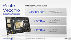
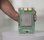
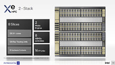
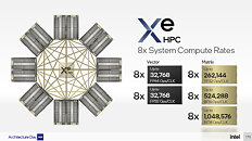
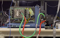
Intel in its 2021 Architecture Day presentation put out fine technical details of its Xe HPC Ponte Vecchio accelerator, including some [very] preliminary performance claims for its current A0-silicon-based prototype. The prototype operates at 1.37 GHz, but achieves out at least 45 TFLOPs of FP32 throughput. We calculated the clock speed based on simple math. Intel obtained the 45 TFLOPs number on a machine running a single Ponte Vecchio OAM (single MCM with two stacks), and a Xeon "Sapphire Rapids" CPU. 45 TFLOPs sees the processor already beat the advertised 19.5 TFLOPs of the NVIDIA "Ampere" A100 Tensor Core 40 GB processor. AMD isn't faring any better, with its production Instinct MI100 processor only offering 23.1 TFLOPs FP32."A0 silicon" is the first batch of chips that come back from the foundry after the tapeout. It's a prototype that is likely circulated within Intel internally, and to a very exclusive group of ISVs and industry partners, under very strict NDAs. It is common practice to ship prototypes with significantly lower clock speeds than what the silicon is capable of, at least to the ISVs, so they can test for functionality and begin developing software for the silicon.Our math for the clock speed is as follows. Intel, in the presentation mentions that each package (OAM) puts out a throughput of 32,768 FP32 ops per clock cycle. It also says that a 2-stack (one package) amounts to 128 Xe-cores, and that each Xe HPC core Vector Engine offers 256 FP32 ops per clock cycle. These add up to 32,768 FP32 ops/clock for one package (a 2-stack). From here, we calculate that 45,000 GFLOPs (measured in clpeak by the way), divided by 32,768 FP32 ops/clock, amounts to 1373 MHz clock speed. A production stepping will likely have higher clock speeds, and throughput scales linearly, but even 1.37 GHz seems like a number Intel could finalize on, given the sheer size and "weight" (power draw) of the silicon (rumored to be 600 W for A0). All this power comes with great thermal costs, with Intel requiring liquid cooling for the OAMs. If these numbers can make it into the final product, then Intel has very well broken through into the HPC space in a big way.



48 Comments on Intel Ponte Vecchio Early Silicon Puts Out 45 TFLOPs FP32 at 1.37 GHz, Already Beats NVIDIA A100 and AMD MI100
The A100 beats the 3090 in pretty much every benchmark across the board by a significant margin. A100 is the top-of-the-top, the $10,000+ NVidia GPU for serious work. Its NVidia's best card.
I don't know where you're getting the bullshit numbers that the 3090 is faster than an A100, but... its just not true. Under any reasonable benchmark, like Linpack, A100 is something like 10-ish TFlops double-precision and 20-ish TFlops single-precision.
The A100 is in a completely different class than the 3090. In FP32 performance even. Its not even close before you factor the 2TBps 80GB HBM2e sitting on the die.
------
Note that the 3090 is lol 1/64th speed FP64. Its terrible at scientific compute. A100 is full speed (well, 1/2 speed, 10 TFlops) of double precision.
My overclocked 3090 is getting 40.6 TFLOPS of single precision (FP32) and only 660GFLOPS of FP64
A100 SM is different from GA102 SM as A100 is more focused on Tensor performance
GA102 SM vs A100 SM
I mean, it's a marvel of engineering and 45 TFlops is a lot, but the A100 was announced in May 2020. Beating a 2 year old card when it's finally going to be released sometime in 2022 sounds somewhat less impressive...
The primary constraint of engineering is time. Money allows for a bigger product to be built, but not necessarily a better product. Given the timeline here, I'm sure the Intel GPU won't be the best. Something weird will happen and not work as expected.
What I'm looking for is a "good first step", not necessarily the best, but a product that shows that Intel knows why NVidia and AMD GPUs have done so well in supercomputing circles. Maybe generation 2 or 3 will be actually competitive.
Though in practice I still assert that the A100 is superior (again, 80GB of 2TBps HBM2e RAM, 10TFlops of double-precision performance, etc. etc.). Almost any GPU-programmer would rather have twice the SMs / cores rather than double the resources spent per SM.
In any case, A100 is still king of NVidia's lineup. Its a few years old however.
Direct Storage decompression on PC is done via Compute Shader (GpGPU) path.
Mesh Shader (similar to Compute Shader) is done on CUDA cores, hence RTX 3090's advantage is shown.3090's TF is real via Compute Shader (GpGPU) path. Pixel Shader path is bottlenecked by raster hardware.Tensor is for pack math INT4, INT8, INT16, and FP16 with FP32 result and it's less flexible than CUDA cores .
Still, competition is always good. It'll be interesting to see how this plays out.
I'm hoping Intel DG2 is 3070 level of performance at 15% less price even if it uses more power, it will sell well if they can build reasonable supply and drivers are stable and updated regularly.
The 3090 runs its fp32 cores at higher clock speeds, and can use its 32-bit integer path to double up the old (Turing) fp32 rate, hence that 36 TFLOPS. But as dragontamer5788 notes, to feed these cores, you need bandwidth. The A100 gets this from its magical but pricey HBM2e; the 3090 forces things by using GDDR6X on a 384-bit bus.
PS: if you think 3090's cost a lot, try to find the price for A100 !!