Report an Error


ATI M86
M86

M86-M

M86-ME

M86-ME XT

Die Shot

Block Diagram
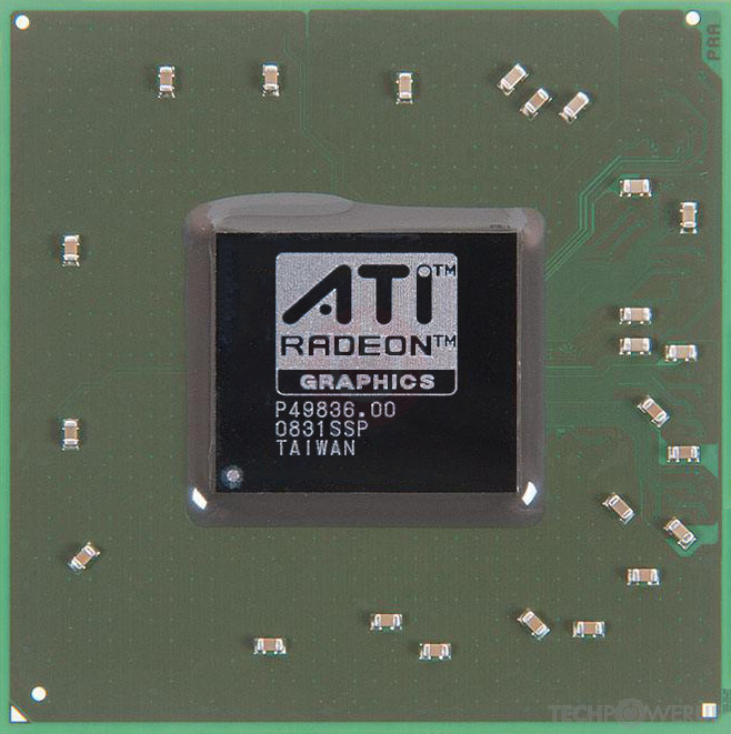
ATI's M86 GPU uses the TeraScale architecture and is made using a 55 nm production process at TSMC. With a die size of 135 mm² and a transistor count of 378 million it is a small chip. M86 supports DirectX 10.1 (Feature Level 10_1). For GPU compute applications, OpenCL version N/A can be used. It features 120 shading units, 8 texture mapping units and 4 ROPs.
Further reading:
R600 Series Instruction Set Architecture 
Graphics Processor
- Released
- Jan 7th, 2008
- GPU Name
- M86
- Desktop Variant
- RV635
- Codename
- Wario
- Architecture
- TeraScale
- Foundry
- TSMC
- Process Size
- 55 nm
- Transistors
- 378 million
- Density
- 2.8M / mm²
- Die Size
- 135 mm²
- Package
- FCBGA-880
Graphics Features
- DirectX
- 10.1 (10_1)
- OpenGL
- 3.3
- OpenCL
- N/A
- Vulkan
- N/A
- Shader Model
- 4.1
- WDDM
- 1.1
- Compute
- GFX3
- DCE
- 3.0
- UVD
- 1.0
Render Config
- Shading Units
- 120
- TMUs
- 8
- ROPs
- 4
- Compute Units
- 3
- Z-Stencil
- 8
- Vertex Cache
- 32 KB
- Texture Cache
- 32 KB
- Tex L1 Cache
- 32 KB per 4 SPs
- L2 Cache
- 128 KB
- Max. TDP
- 30 W
All TeraScale GPUs
- ATI M72
- ATI M74
- ATI M76
- ATI M82
- ATI M84
- ATI M86
- ATI M88
- ATI M92
- AMD M93
- ATI M93
- ATI M96
- ATI M97
- ATI M98
- ATI R600
- ATI R680
- ATI R700
- ATI RS780
- ATI RS880
- ATI RV610
- ATI RV620
- ATI RV630
- ATI RV635
- ATI RV670
- AMD RV670
- ATI RV710
- AMD RV711
- ATI RV711
- ATI RV730
- ATI RV740
- ATI RV770
- AMD RV770
- ATI RV790
- ATI RX881
- ATI Theater 650 PRO
- ATI Xenos Corona
- ATI Xenos Falcon
- ATI Xenos Jasper
- ATI Xenos Vejle
- ATI Xenos Xenon
ATI GPU Architecture History
Graphics cards using the ATI M86 GPU
| Name | Chip | Memory | Shaders | TMUs | ROPs | GPU Clock | Memory Clock |
|---|---|---|---|---|---|---|---|
| M86-ME | 512 MB | 120 | 8 | 4 | 500 MHz | 700 MHz | |
| M86-ME XT | 256 MB | 120 | 8 | 4 | 680 MHz | 800 MHz | |
| M86-M GL | 512 MB | 120 | 8 | 4 | 600 MHz | 700 MHz | |
| M86-ME XT GL | 256 MB | 120 | 8 | 4 | 680 MHz | 800 MHz |


M86 GPU Notes
| Desktop Variant: RV635 Codename: Wario Graphics/Compute: GFX3 Display Core Engine: 3.0 Unified Video Decoder: 1.0 Chip Codes: 216-0683008 - M86-M / M86-M LP / M86-M GL 216-0683013 - M86-ME / M86-ME LP 216-0683010 - M86-ME XT / M86-ME XT GL |
Jun 30th, 2024 10:38 EDT
change timezone
Latest GPU Drivers
New Forum Posts
- Monitor randomly goes black / blinks for a second then comes back (9)
- Power Supply Buying Guide (15)
- Memory Mhz importance. (22)
- Your PC ATM (34667)
- FFXIV Dawntrail has one of the worst stories in video game history. Literally makes no sense. 0/10 (1)
- Can anyone figure out what's wrong with my laptop? (15)
- A silly though concerning case fans (0)
- The TPU UK Clubhouse (24898)
- Package C8 State vs C10 State Regarding Battery Performance (1)
- Best microATX case? (22)
Popular Reviews
- Endgame Gear OP1 8K Review
- Corsair MP600 Mini 2 TB Review - Great Storage for Steam Deck
- Bykski CPU-FIRE-ON-I CPU Water Block Review
- Lian Li HydroShift LCD 360S AIO Review
- XPG Invader X Review
- Upcoming Hardware Launches 2024 (Updated May 2024)
- XFX Radeon RX 7900 XTX Magnetic Air Review
- Sapphire Radeon RX 7600 XT Pulse Review
- AMD Ryzen 7 7800X3D Review - The Best Gaming CPU
- Patriot Viper Xtreme 5 DDR5-7600 32 GB CL36 Review
Controversial News Posts
- AMD Outs Ryzen 5000XT Processors for Socket AM4, an 8-year Old Socket (208)
- Legendary Overclocker KINGPIN Leaves EVGA and Joins PNY to Develop Next-Generation GPUs for Extreme OC (195)
- AMD Says Ryzen 9000 Series Won't Beat 7000X3D Series at Gaming (140)
- Possible Specs of NVIDIA GeForce "Blackwell" GPU Lineup Leaked (139)
- First Reviews are Live and Snapdragon X Elite Doesn't Quite Deliver on Promised Performance (124)
- ASUS Enhances Customer Support Following Gamers Nexus Investigation (118)
- Nightmare Fuel for Intel: Arm CEO Predicts Arm will Take Over 50% Windows PC Market-share by 2029 (112)
- AMD Zen 5 Storms into Gaming Desktops with Ryzen 9000 "Granite Ridge" Processors (100)