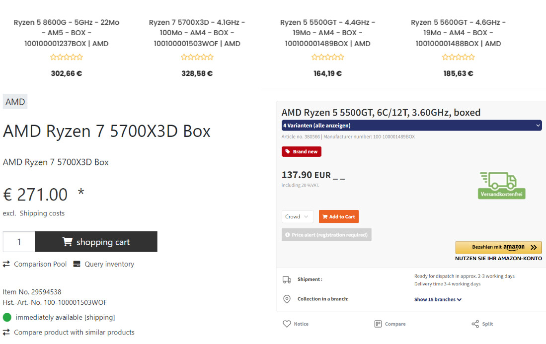
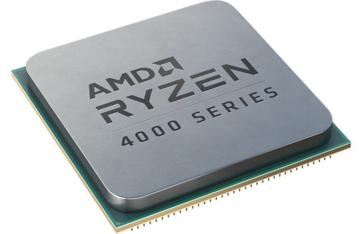
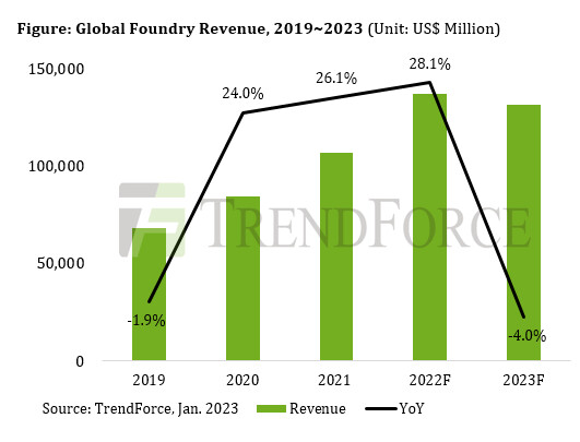
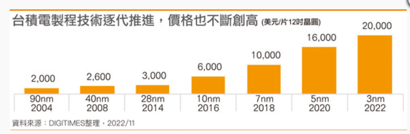
AMD Ryzen 7 5700X3D and 5000GT Chips Start Selling in Europe
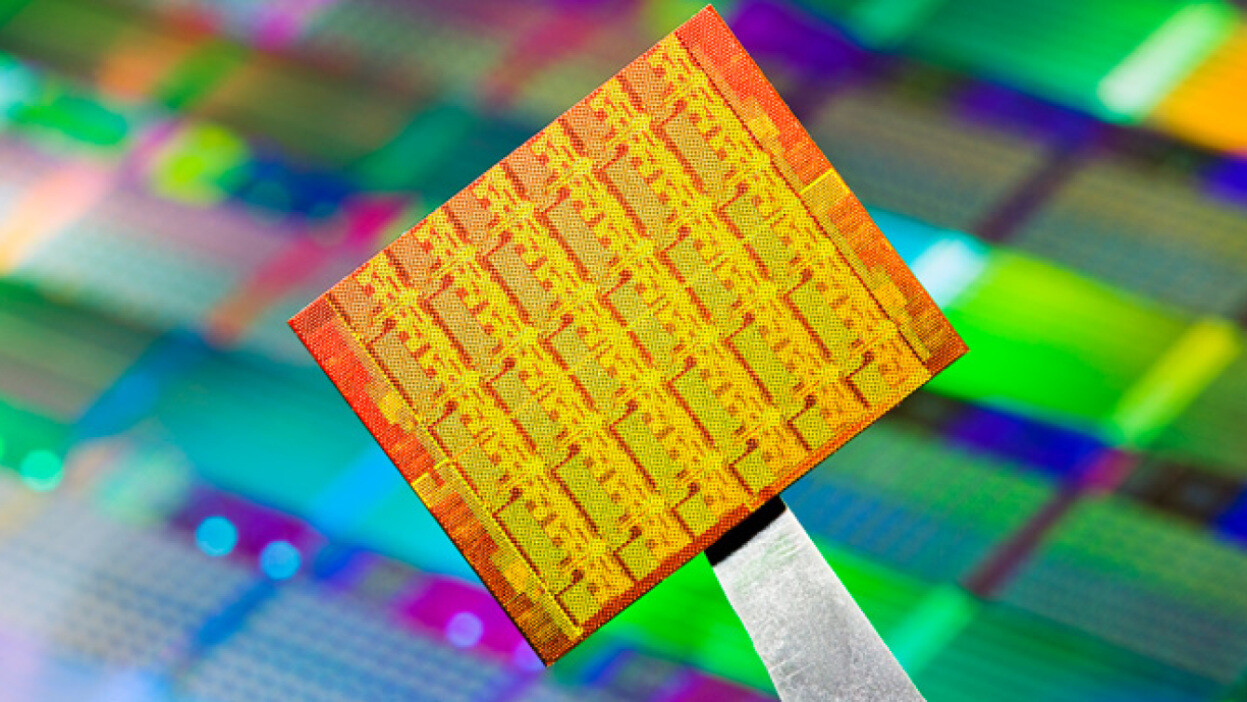
The AMD Socket AM4 platform is still alive and kicking, with AMD releasing new processor models in its 7th year. Many of these chips started selling online in Europe. The Ryzen 7 5700X3D is a slightly lower clocked version of the 5800X3D, which for many of those still on AM4 is the final upgrade to their platform. The 5800X3D may be based on the older "Zen 3" microarchitecture, but thanks to its 3D Vertical Cache technology, offers gaming performance comparable to the Core i9-12900K "Alder Lake," making even 7-year old AM4 gaming desktops contemporary. To cash in on this exact market, AMD released a more cost-effective option, the Ryzen 7 5700X3D.
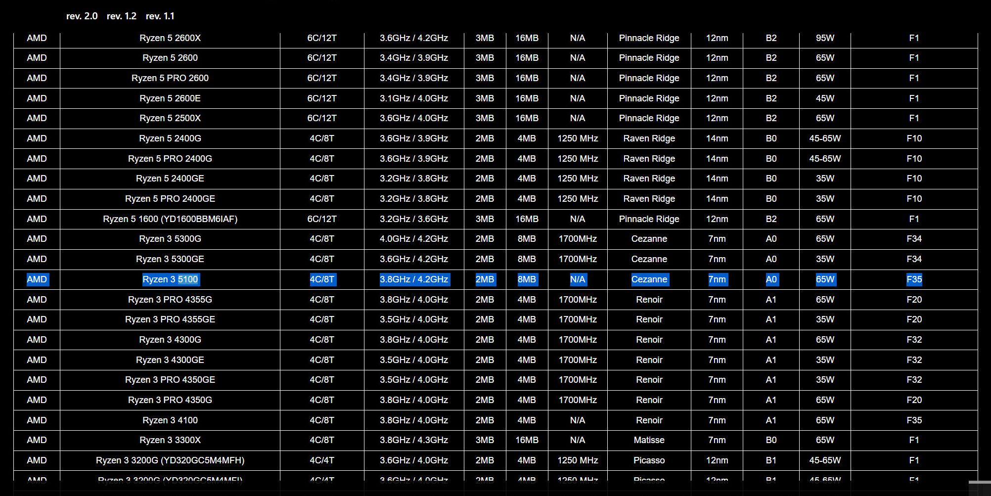
The 5700X3D is an 8-core/16-thread Socket AM4 processor that features 96 MB of L3 cache thanks to the 3D V-cache technology, just like the 5800X3D, but comes with a maximum boost frequency of 4.10 GHz, compared to the 4.50 GHz of the 5800X3D. Store listings do not mention its TDP or base frequency. The 5700X3D is being listed at 271€ including taxes, or about 15-20% cheaper than the 5800X3D. A word of caution when choosing the 5700X3D would be its close to non-existent overclocking headroom, so this probably isn't a chip that you can manually overclock to performance levels of a 5800X3D while saving some 40€ on the side.
The 5700X3D is an 8-core/16-thread Socket AM4 processor that features 96 MB of L3 cache thanks to the 3D V-cache technology, just like the 5800X3D, but comes with a maximum boost frequency of 4.10 GHz, compared to the 4.50 GHz of the 5800X3D. Store listings do not mention its TDP or base frequency. The 5700X3D is being listed at 271€ including taxes, or about 15-20% cheaper than the 5800X3D. A word of caution when choosing the 5700X3D would be its close to non-existent overclocking headroom, so this probably isn't a chip that you can manually overclock to performance levels of a 5800X3D while saving some 40€ on the side.