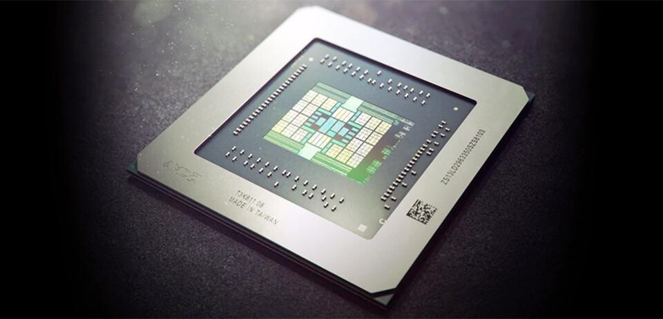
AMD Ryzen 5 4400G Desktop "Renoir" 6-core APU Put Through 3DMark11
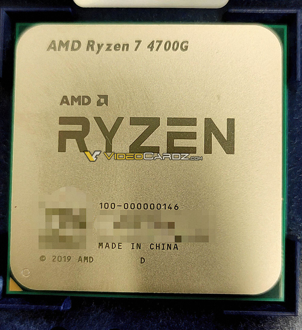
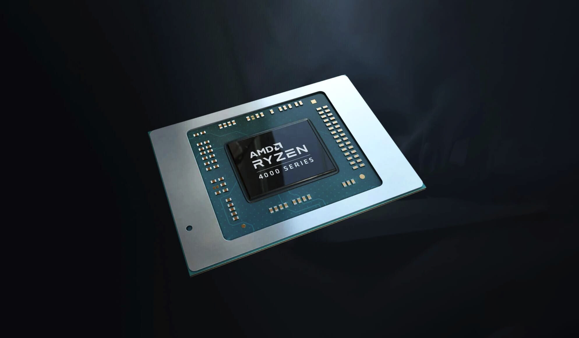
It looks like AMD's Ryzen 4000G line of socket AM4 desktop APUs based on the 8-core 7 nm "Renoir" silicon will be a lot wider than just a couple of SKUs. We've seen plenty of material on the top Ryzen 7 4700G part that maxes out everything on the silicon, along with increased power limits and clock speeds. It looks like the Ryzen 5 4000G series will consist of 6-core/12-thread parts. One such chip, the Ryzen 5 4400G surfaced on the 3DMark database, as dug up by TUM_APISAK. They earlier brought you a 3DMark score comparison between the 4400G, the top 4700G, and the entry-level 4200G.
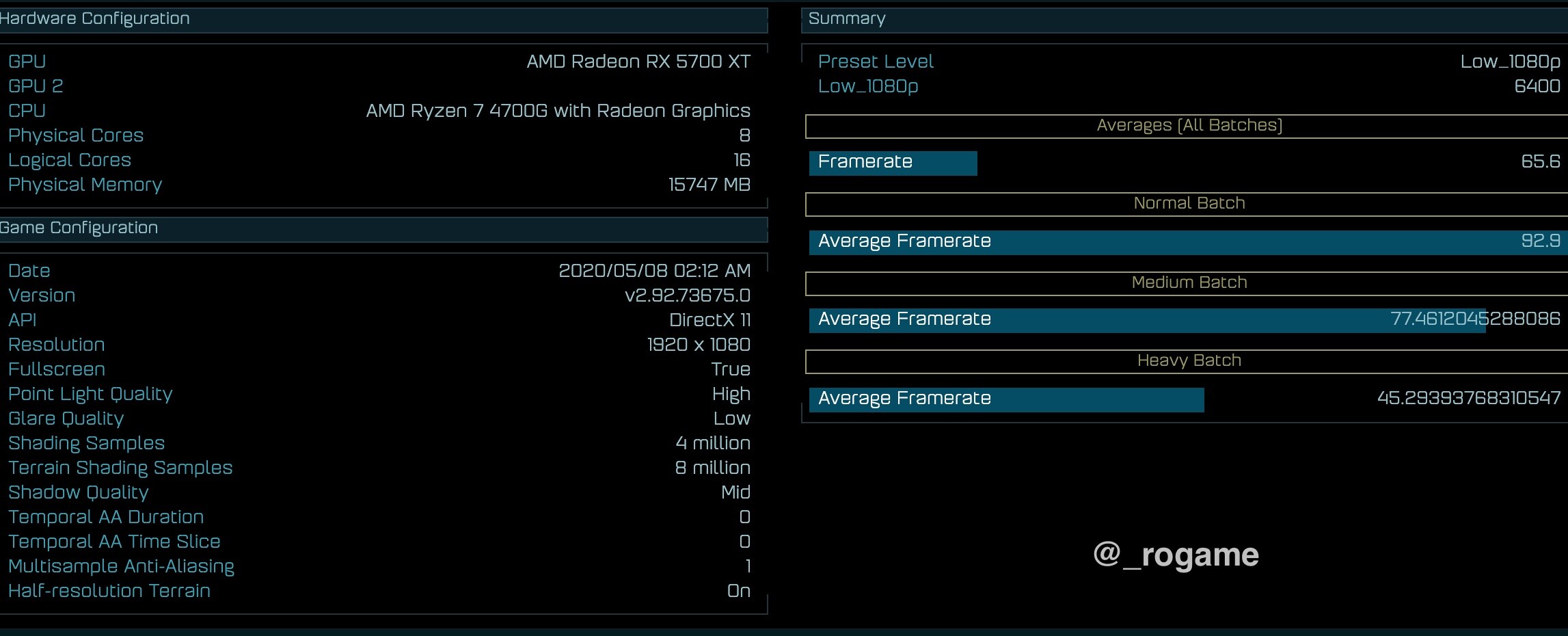
The Ryzen 5 4400G (possible OPN: 100-000000143) appears to be a 6-core/12-thread part based on "Renoir," with the CPU clocked at 3.70 GHz base and possibly 4.30 GHz boost. The "Vega" NGCU count of the iGPU is unknown, but its engine clock is set at 1.90 GHz (max). With the "P" (performance) preset, the 4400G allegedly scores 4395 points in the 3DMark 11 graphics test suite (graphics score); with 10241 points physics score.
The Ryzen 5 4400G (possible OPN: 100-000000143) appears to be a 6-core/12-thread part based on "Renoir," with the CPU clocked at 3.70 GHz base and possibly 4.30 GHz boost. The "Vega" NGCU count of the iGPU is unknown, but its engine clock is set at 1.90 GHz (max). With the "P" (performance) preset, the 4400G allegedly scores 4395 points in the 3DMark 11 graphics test suite (graphics score); with 10241 points physics score.