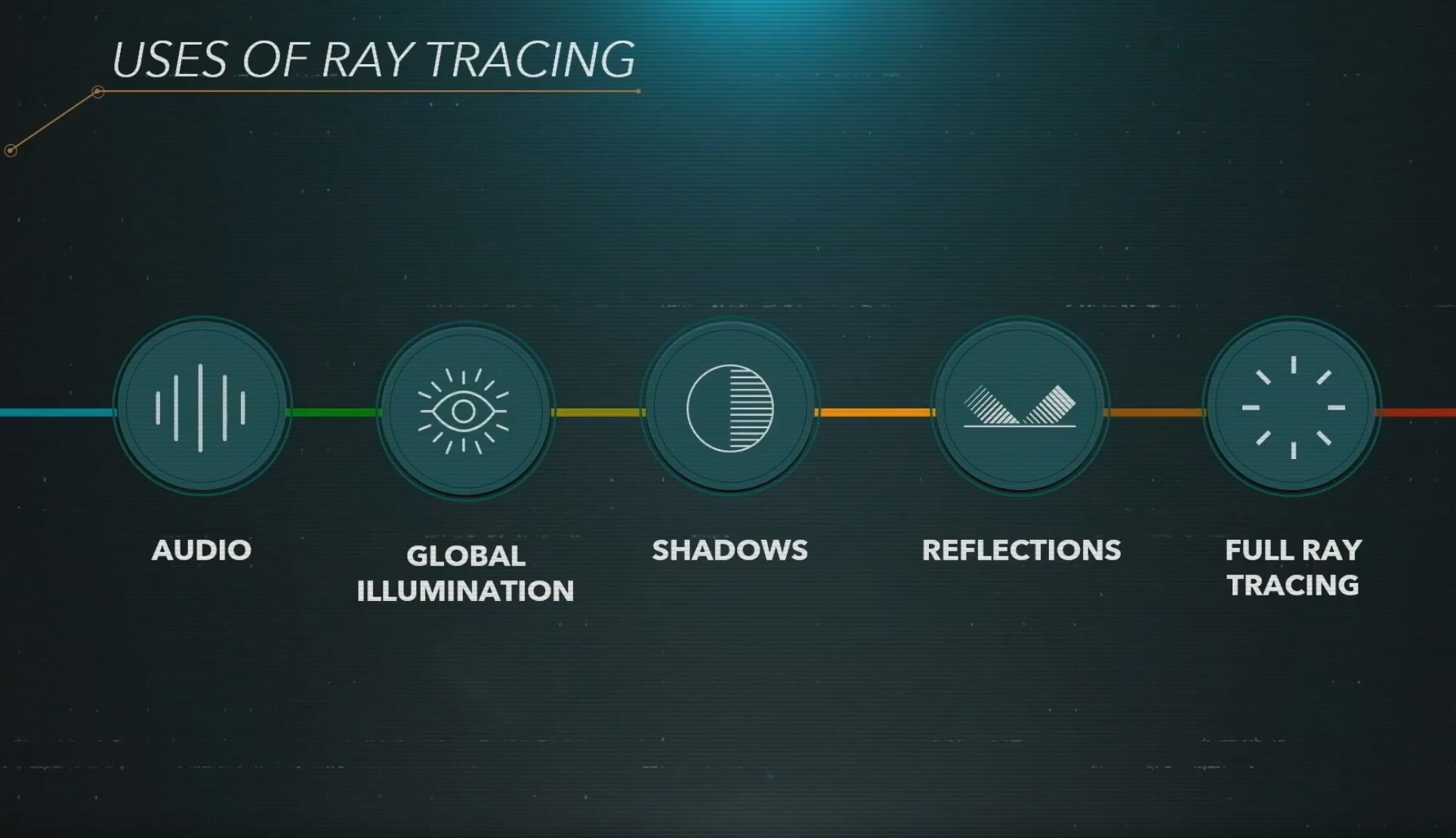
AMD 4th Gen Ryzen Desktop Processors to Launch Around September 2020
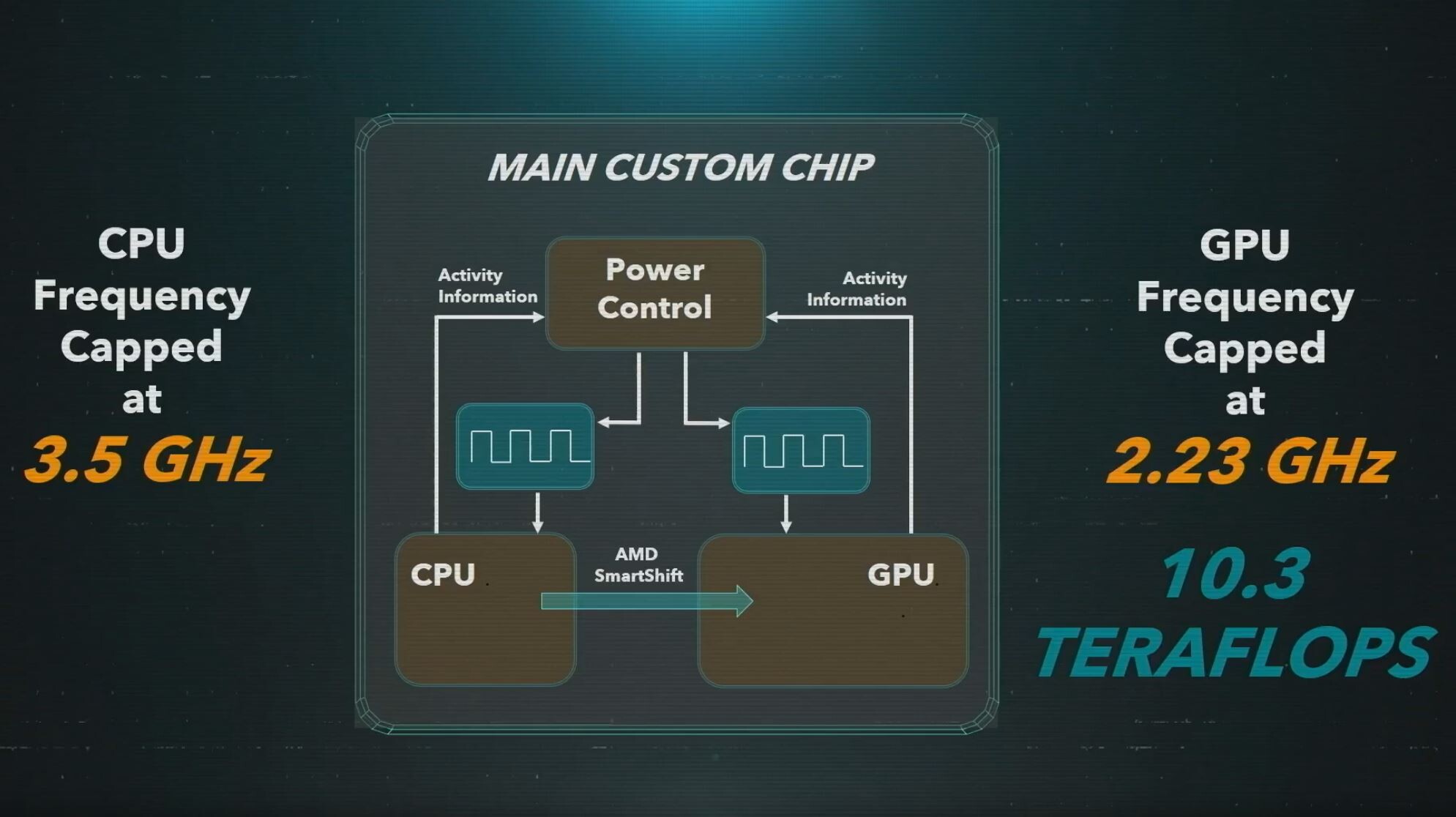
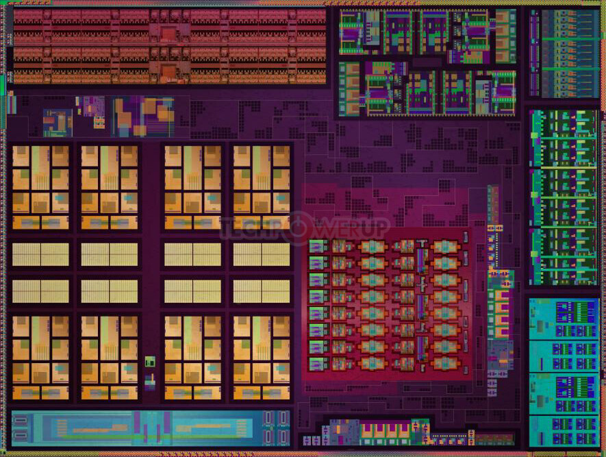
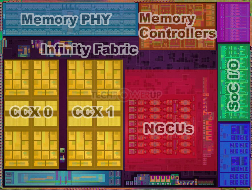
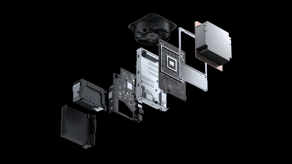
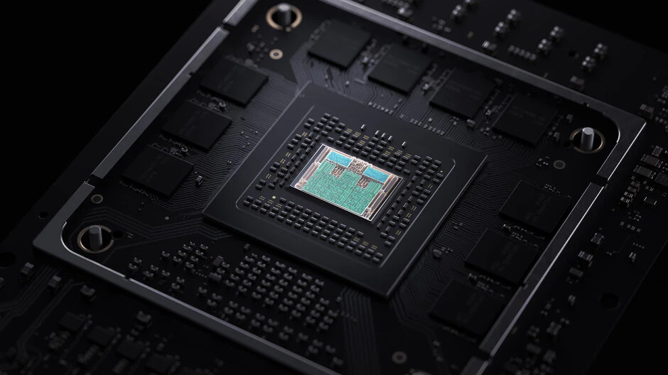
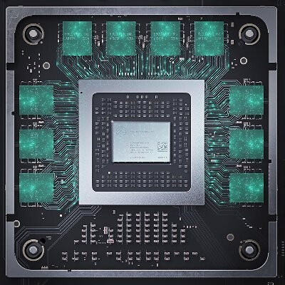
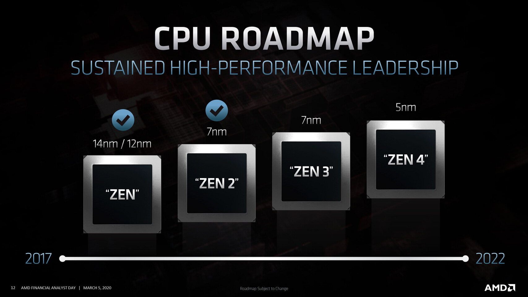
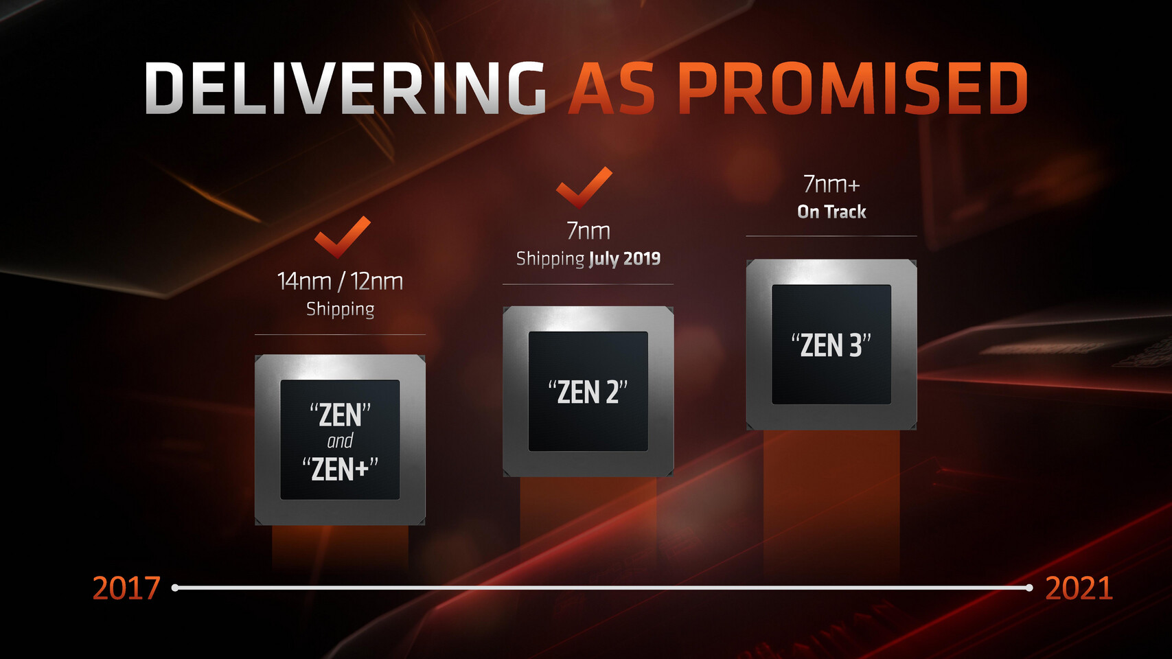
AMD's 4th generation Ryzen desktop processors are expected to launch around September 2020, sources in the motherboard industry tell DigiTimes. Codenamed "Vermeer," successor to "Matisse," these processors will be socket AM4 multi-chip modules of up to two CPU complex dies based on the "Zen 3" microarchitecture, combined with an I/O controller die. The "Zen 3" chiplets are expected to be fabricated on a newer 7 nm-class process by TSMC, either N7P or N7+. The biggest design change with "Zen 3" is the doing away of CCX arrangement of CPU cores, with each chiplet holding a common block of cores sharing a last-level cache. This, along with clock speed headroom gains from the new node are expected to yield generational price-performance increases.
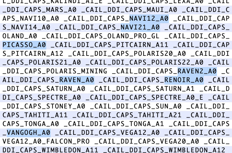
The "Zen 2" based 8-core "Renoir" die is also expected to make its socket AM4 debut within 2020, succeeding the "Picasso" based quad-core Ryzen 3000-series APUs. This is a particularly important product for AMD, as it is expected to compete with Intel's 10th generation Core i5 6-core/12-thread processors in terms of pricing, while offering more cores (8-core/16-thread) and a faster iGPU. The 4th gen Ryzen socket AM4 processor lineup will launch alongside AMD's 600-series motherboard chipset, with forwards- and backwards-compatibility (i.e., "Vermeer" and "Renoir" working with older chipsets, and older AM4 processors working on 600-series chipset motherboards). AMD was originally expected to unveil these processors at the 2020 Computex trade-show in June, but Computex itself is rescheduled to late-September.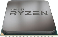
The "Zen 2" based 8-core "Renoir" die is also expected to make its socket AM4 debut within 2020, succeeding the "Picasso" based quad-core Ryzen 3000-series APUs. This is a particularly important product for AMD, as it is expected to compete with Intel's 10th generation Core i5 6-core/12-thread processors in terms of pricing, while offering more cores (8-core/16-thread) and a faster iGPU. The 4th gen Ryzen socket AM4 processor lineup will launch alongside AMD's 600-series motherboard chipset, with forwards- and backwards-compatibility (i.e., "Vermeer" and "Renoir" working with older chipsets, and older AM4 processors working on 600-series chipset motherboards). AMD was originally expected to unveil these processors at the 2020 Computex trade-show in June, but Computex itself is rescheduled to late-September.