News Posts matching #7 nm

Return to Keyword Browsing

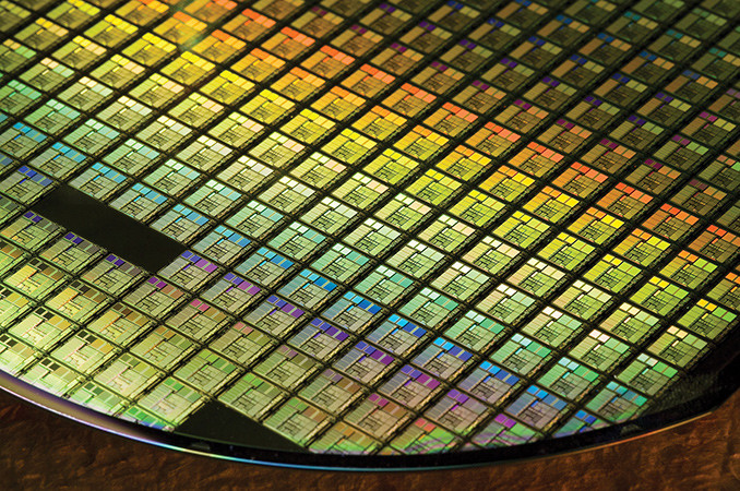
TSMC Trembles Under 7 nm Product Orders, Increases Delivery Lead Times Threefold - Could Hit AMD Product Availability

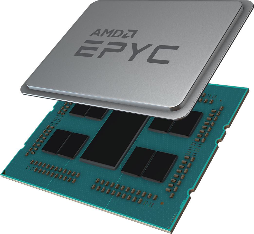
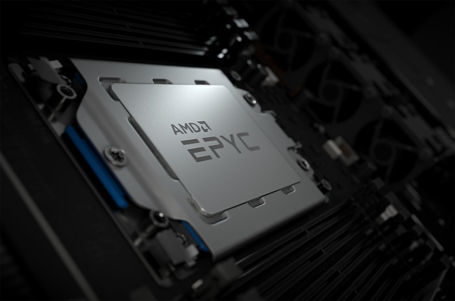
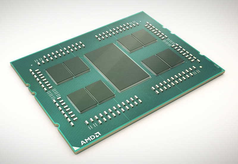
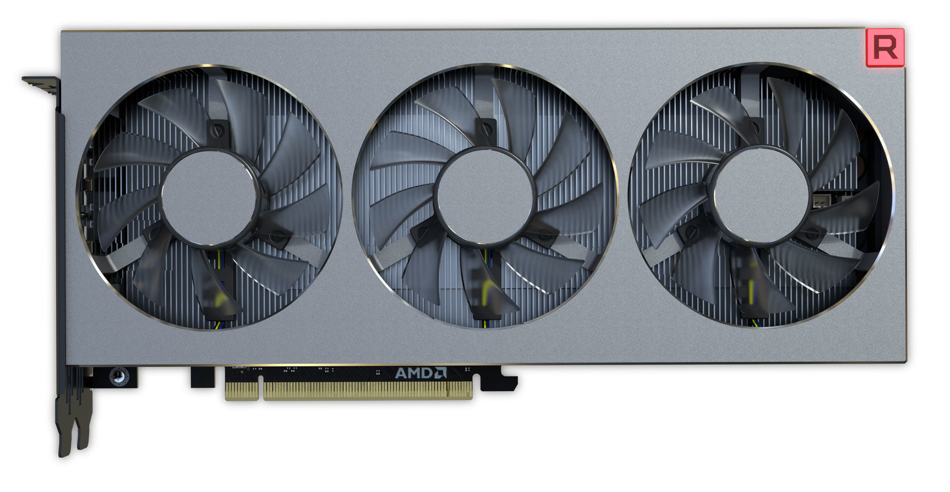
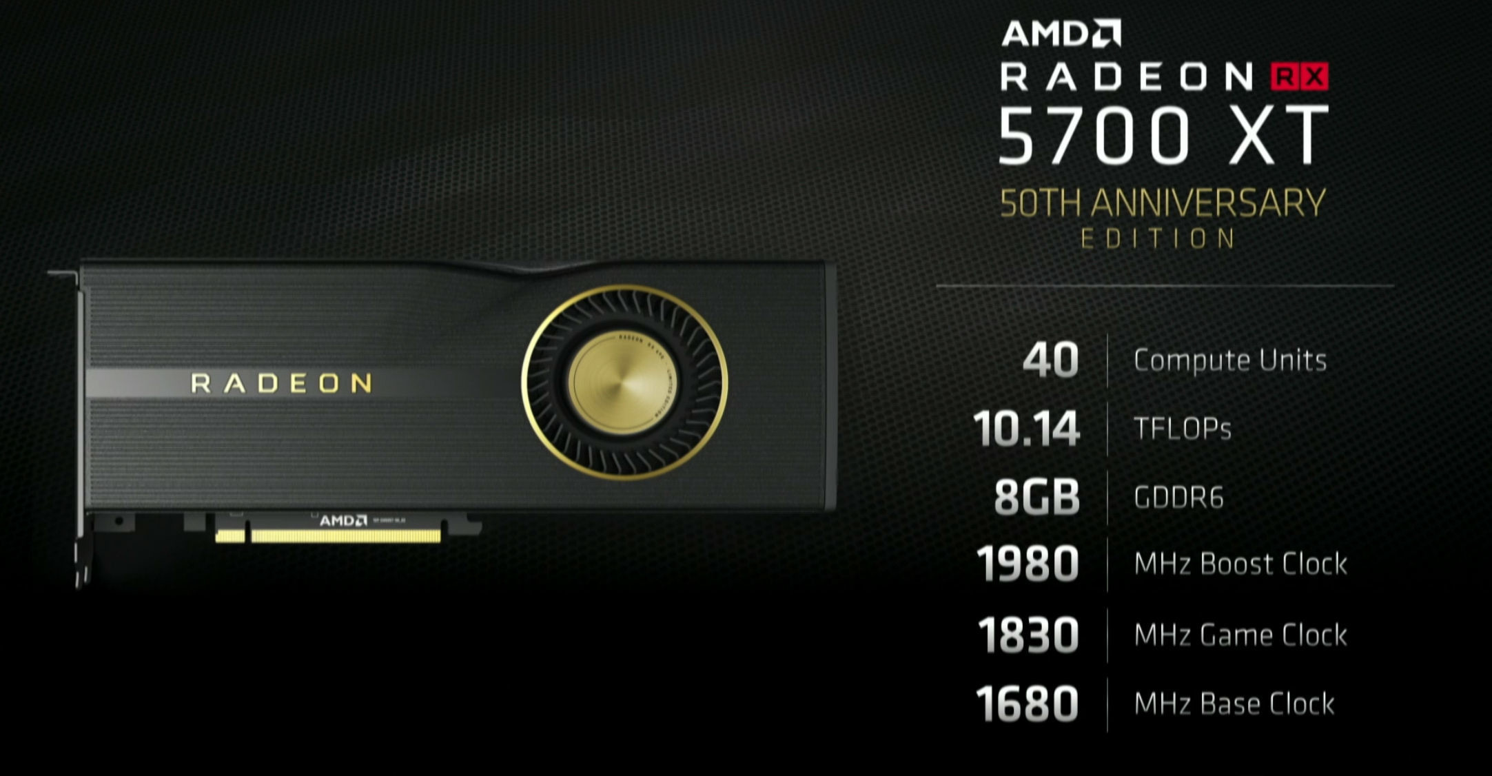
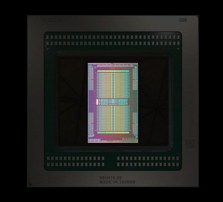
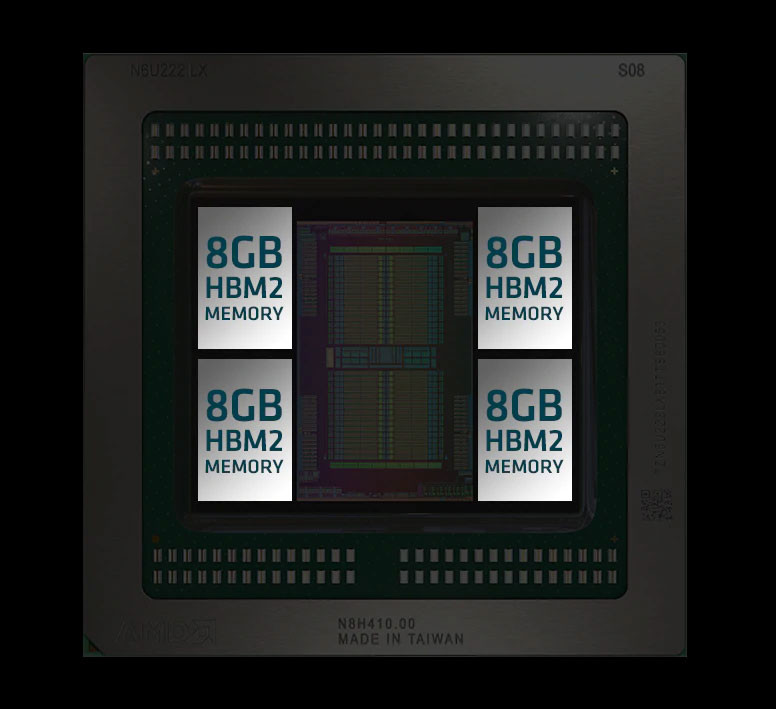
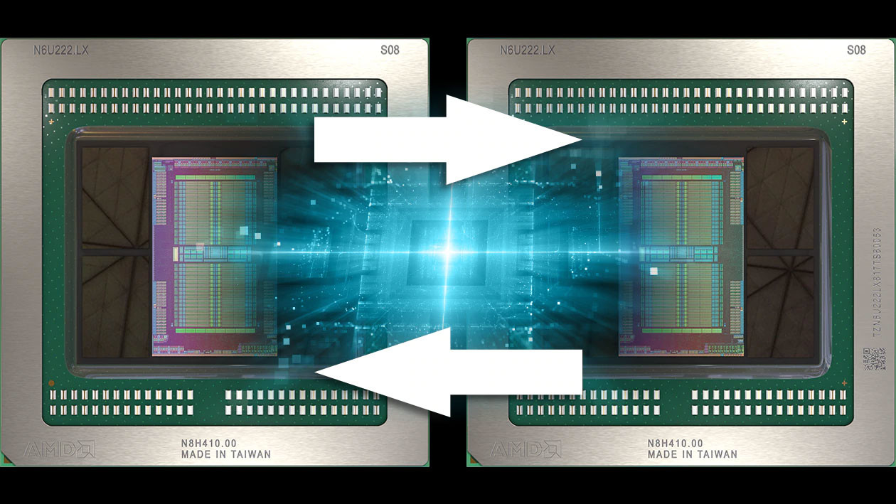
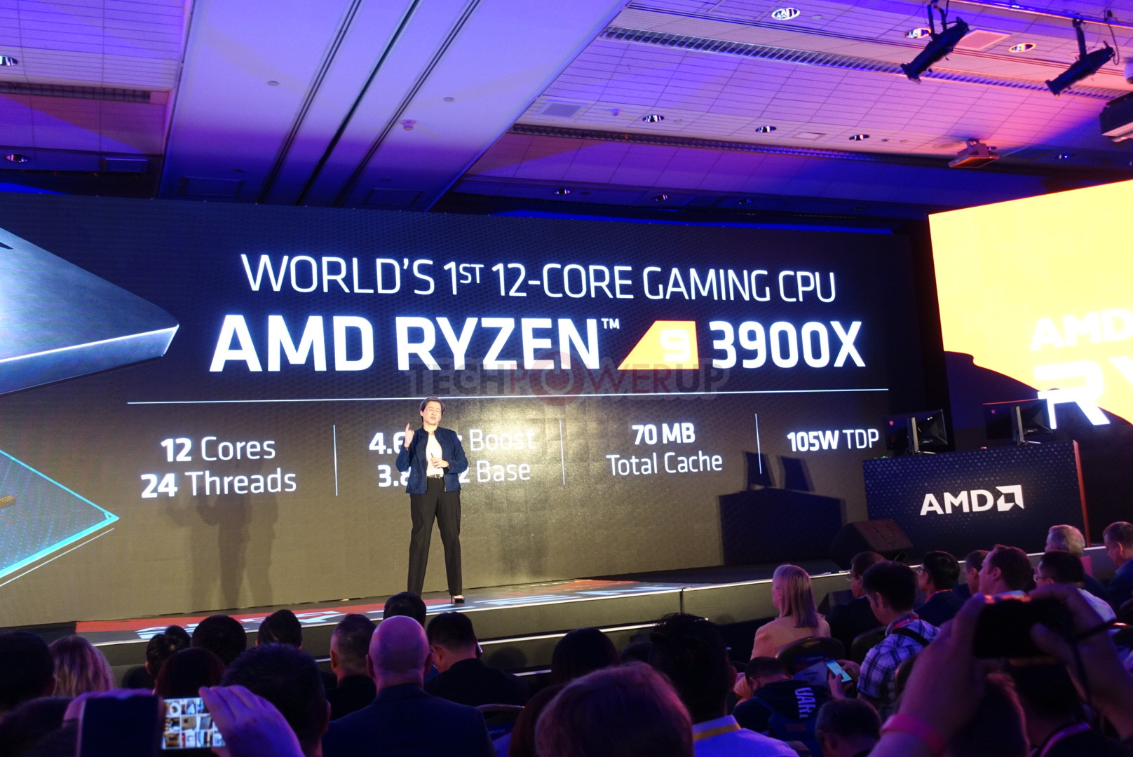
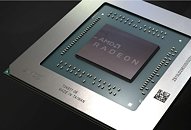
TSMC is on the vanguard of chipset fabrication technology at this exact point in time - its 7 nm technology is the leading-edge of all large volume processes, and is being tapped by a number of companies for 7 nm silicon. One of its most relevant clients for our purposes, of course, is AMD - the company now enjoys a fabrication process lead over arch-rival Intel much due to its strategy of fabrication spin-off and becoming a fabless designer of chips. AMD's current product stack has made waves in the market by taking advantage of 7 nm's benefits, but it seems this may actually become a slight problem in the not so distant future.

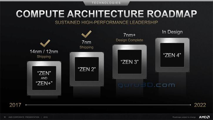
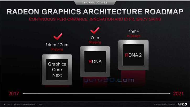
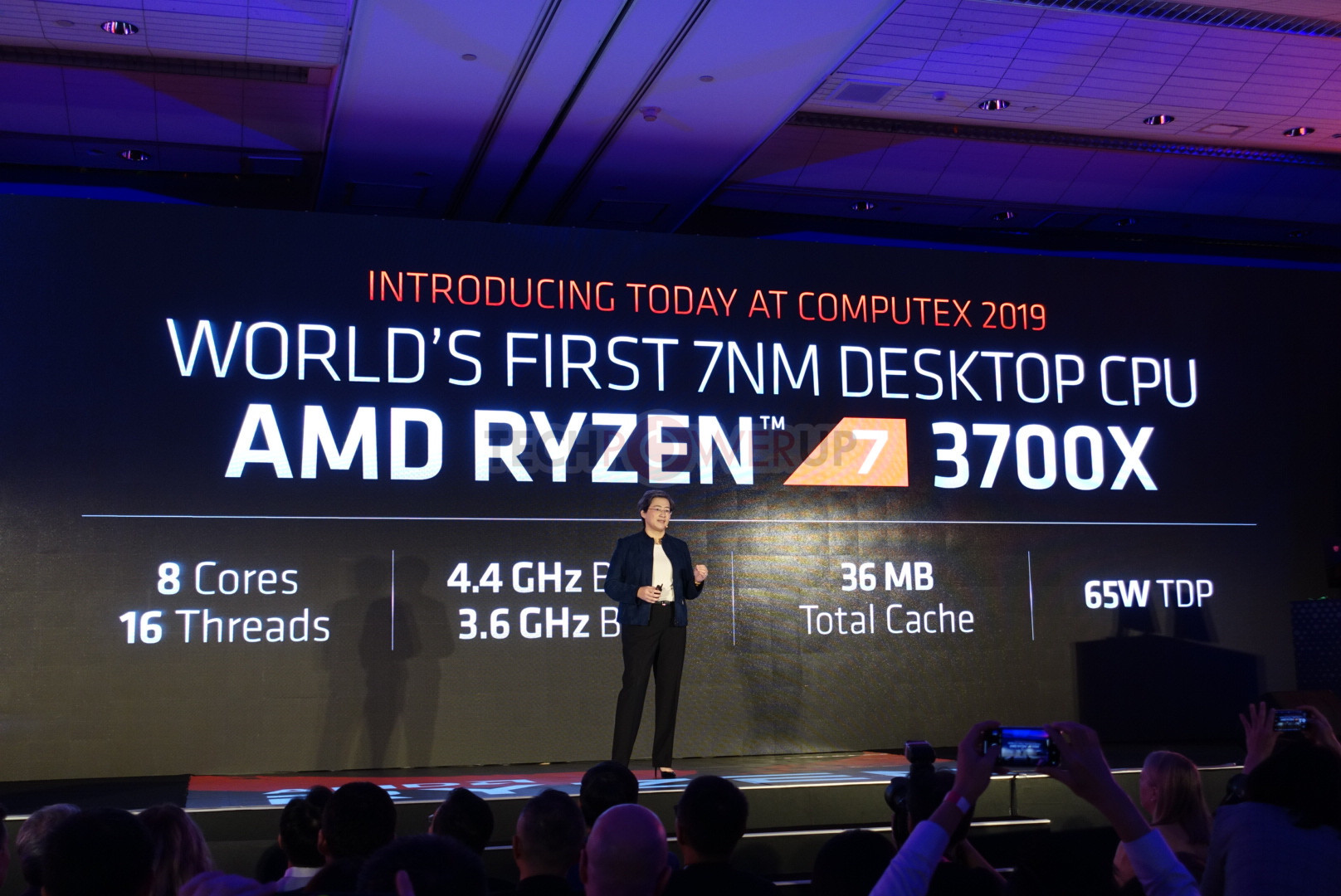
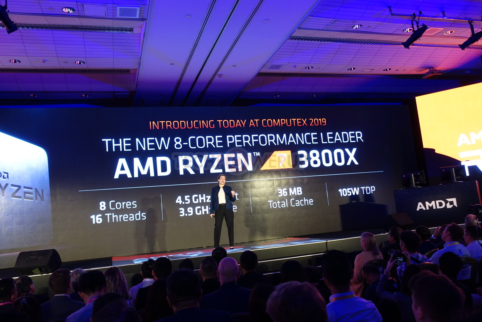
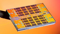
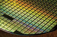
TSMC has announced a threefold increase in its delivery lead times for 7 nm orders, from two months to nearly six months, which means that orders will now have to wait three times longer to be fulfilled than they once did. This means that current channel supplies and orders made after the decision from TSMC will take longer to materialize in actual silicon, which may lead to availability slumps should demand increase or maintain. AMD has its entire modern product stack built under the 7 nm process, so this could potentially affect both CPUs and GPUs from the company - and let's not forget AMD's Zen 3 and next-gen RDNA GPUs which are all being designed for the 7 nm+ process node. TSMC is expected to set aside further budget to expand capacity of its most advanced nodes, whilst accelerating investment on their N7+, N6, N5, and N3 nodes.

AMD Readies the Low-Power "Dali" APU for Thin-and-Light Notebooks

AMD is expected to bring back its low-power APU family in 2020 with the new "Dali" silicon. Updated company roadmap slides see the inclusion of "Dali" as a "value mobile APU," positioned under "Renoir," a performance APU targeting both the mainstream notebook and desktop (socket AM4) platforms. AMD looks keen to branch out its APU business in two directions.

"Renoir" is expected to be a "Zen 2" based APU with CPU performance matching at least the Ryzen 5 3600 or 3700X, and a faster "Vega" based iGPU. It wouldn't surprise us if "Dali" is a monolithic 7 nm die with two "Zen 2" CPU cores and a tiny iGPU with 3-4 compute units. "Renoir," on the other hand, could be an MCM with an 8-core "Zen 2" chiplet and an enlarged I/O controller die that has the iGPU. "Dali" could see the light of the day only in 2020, by which time TSMC could substantially increase its 7 nm volumes and clear the decks for its new 7 nm EUV mass-production.

AMD Updates Roadmaps to Lock RDNA2 and Zen 3 onto 7nm+, with 2020 Launch Window

AMD updated its technology roadmaps to reflect a 2020 launch window for its upcoming CPU and graphics architectures, "Zen 3" and RDNA2. The two will be based on 7 nm+ , which is AMD-speak for the 7 nanometer EUV silicon fabrication process at TSMC, that promises a significant 20 percent increase in transistor-densities, giving AMD high transistor budgets and more clock-speed headroom. The roadmap slides however hint that unlike the "Zen 2" and RDNA simultaneous launch on 7th July 2019, the next-generation launches may not be simultaneous.

The slide for CPU microarchitecture states that the design phase of "Zen 3" is complete, and that the microarchitecture team has already moved on to develop "Zen 4." This means AMD is now developing products that implement "Zen 3." On the other hand, RDNA2 is still in design phase. The crude x-axis on both slides that denotes year of expected shipping, too appears to suggest that "Zen 3" based products will precede RDNA2 based ones. "Zen 3" will be AMD's first response to Intel's "Comet Lake-S" or even "Ice Lake-S," if the latter comes to fruition before Computex 2020. In the run up to RDNA2, AMD will scale up RDNA a notch larger with the "Navi 12" silicon to compete with graphics cards based on NVIDIA's "TU104" silicon. "Zen 2" will receive product stack additions in the form of a new 16-core Ryzen 9-series chip later this month, and the 3rd generation Ryzen Threadripper family.

AMD "Renoir" APU to Support LPDDR4X Memory and New Display Engine

AMD's next-generation "Renoir" APU, which succeeds the company's 12 nm "Picasso," will be the company's truly next-generation chip to feature an integrated graphics solution. It's unclear as of now, if the chip will be based on a monolithic die, or if it will be a multi-chip module of a 7 nm "Zen 2" chiplet paired with an enlarged I/O controller die that has the iGPU. We're getting confirmation on two key specs - one, that the iGPU will be based on the older "Vega" graphics architecture, albeit with an updated display engine to support the latest display standards; and two, that the processor's memory controller will support the latest LPDDR4X memory standard, at speeds of up to 4266 MHz DDR. In comparison, Intel's "Ice Lake-U" chip supports LPDDX4X up to 3733 MHz.

Code-lines pointing toward "Vega" graphics with an updated display controller mention the new DCN 2.1, found in AMD's new "Navi 10" GPU. This controller supports resolutions of up to 8K, DSC 1.2a, and new resolutions of 4K up to 240 Hz and 8K 60 Hz over a single cable, along with 30 bits per pixel color. The multimedia engine is also suitably updated to VCN 2.1 standard, and provides hardware-accelerated decoding for some of the newer video formats, such as VP9 and H.265 at up to 90 fps at 4K, and 8K up to 24 fps, and H.264 up to 150 fps at 4K. There's no word on when "Renoir" comes out, but a 2020 International CES unveil is likely.

AMD Designing Zen 4 for 2021, Zen 3 Completes Design Phase, out in 2020

AMD in its 2nd generation EPYC processor launch event announced that it has completed the design phase of its next-generation "Zen 3" CPU microarchitecture, and is currently working on its successor, the "Zen 4." AMD debuted its "Zen 2" microarchitecture with the client-segment 3rd generation Ryzen desktop processor family, it made its enterprise debut with the 2nd generation EPYC. This is the first x86 CPU microarchitecture designed for the 7 nanometer silicon fabrication process, and is being built on a 7 nm DUV (deep ultraviolet) node at TSMC. It brings about double-digit percentage IPC improvements over "Zen+."

The "Zen 3" microarchitecture is designed for the next big process technology change within 7 nm, EUV (extreme ultraviolet), which allows significant increases in transistor densities, and could facilitate big improvements in energy-efficiency that could be leveraged to increase clock-speeds and performance. It could also feature new ISA instruction-sets. With "Zen 3" passing design phase, AMD will work on prototyping and testing it. The first "Zen 3" products could debut in 2020. "Zen 4" is being designed for a different era.

2nd Gen AMD EPYC Processors Set New Standard for the Modern Datacenter

At a launch event today, AMD was joined by an expansive ecosystem of datacenter partners and customers to introduce the 2nd Generation AMD EPYC family of processors that deliver performance leadership across a broad number of enterprise, cloud and high-performance computing (HPC) workloads. 2nd Gen AMD EPYC processors feature up to 64 "Zen 2" cores in leading-edge 7 nm process technology to deliver record-setting performance while helping reduce total cost of ownership (TCO) by up to 50% across numerous workloads. At the event, Google and Twitter announced new 2nd Gen AMD EPYC processor deployments and HPE and Lenovo announced immediate availability of new platforms.

"Today, we set a new standard for the modern datacenter with the launch of our 2nd Gen AMD EPYC processors that deliver record-setting performance and significantly lower total cost of ownership across a broad set of workloads," said Dr. Lisa Su, president and CEO, AMD. "Adoption of our new leadership server processors is accelerating with multiple new enterprise, cloud and HPC customers choosing EPYC processors to meet their most demanding server computing needs."

AMD Zen 2 EPYC "Rome" Launch Event Live Blog

AMD invited TechPowerUp to their launch event and editor's day coverage of Zen 2 EPYC processors based on the 7 nm process. The event was a day-long affair which included product demos and tours, and capped off with an official launch presentation which we are able to share with you live as the event goes on. Zen 2 with the Ryzen 3000-series processors ushered in a lot of excitement, and for good reason too as our own reviews show, but questions remained on how the platform would scale to the other end of the market. We already knew, for example, that AMD secured many contracts based on their first-generation EPYC processors, and no doubt the IPC increase and expected increased core count would cause similar, if not higher, interest here. We also expect to know shortly about the various SKUs and pricing involved, and also if AMD wants to shed more light on the future of the Threadripper processor family. Read below, and continue past the break, for our live coverage.
21:00 UTC: Lisa Su is on the stage at the Palace of Fine Arts events venue in San Francisco to present AMD's latest developments on EPYC for datacenters, using the Zen 2 microarchitecture.

21:10 UTC: AMD focuses not just on delivering a single chip, but it's goal is to deliver a complete solution for the enterprise.

AMD Could Launch New Navi GPUs Soon

AMD's president and CEO Dr. Lisa Su was talking during AMD's Q2 earnings Q&A conference and got asked a very interesting question. When prompted about high end Navi GPUs, Dr. Su answered with "I would say they are coming. You should expect that our execution on those are on track and we have a rich 7 nm portfolio beyond the products that we have already announced in the upcoming quarters."

This answer gives us hope to see more powerful Navi GPUs possibly by the end of the year, meaning that AMD's answer to Turing is almost ready. As we saw earlier in the rumors, we might get additional higher end GPU models in form of alleged RX 5800 and RX 5900, with XT variants available for both of those models. The RX 5800 is supposed to utilize a new GPU core called Navi 12, while the core for RX 5900 is still unknown.

AMD 3rd Gen Threadripper Coming This October to Take on Intel's New HEDT Lineup?

AMD is planning to surprise Intel by unveiling its 3rd generation Ryzen Threadripper HEDT (high-end desktop) processor lineup around the same time Intel launches its 10th generation Core "Cascade Lake-X" processor and the "Glacial Falls" HEDT platform, according to sources in the motherboard industry, speaking with DigiTimes. We're fairly sure the sources aren't referring to AMD's 16-core Ryzen 9 3950X processor, because it has already been announced and will be available in September.

The 3rd generation Ryzen Threadripper will likely be a derivative of the company's "Rome" multi-chip module, and compatible with existing socket TR4 motherboards with a BIOS update, although a new chipset could also be launched to enable PCI-Express gen 4.0. AMD has the option to deploy up to 64 CPU cores across eight 7 nm "Zen 2" chiplets, while the 12 nm I/O controller die will be likely reconfigured for the HEDT platform with a monolithic 4-channel DDR4 memory interface and 64 PCIe gen 4.0 lanes. It's capable of 8 memory channels on the 2nd generation EPYC.

Intel's CEO Blames 10 nm Delay on being "Too Aggressive"

During Fortune's Brainstorm Tech conference in Aspen, Colorado, Intel's CEO Bob Swan took stage and talked about the company, about where Intel is now and where they are headed in the future and how the company plans to evolve. Particular focus was put on how Intel became "data centric" from "PC centric," and the struggles it encountered.

However, when asked about the demise of Moore's Law, Swan detailed the aggressiveness that they approached the challenge with. Instead of the regular two times improvement in transistor density every two years, Swan said that Intel has always targeted better and greater densities so that it would stay the leader in the business.

EK Launches EK-Vector Special Edition RX 5700-series Water Blocks

EK Water Blocks, the leading premium computer liquid cooling gear manufacturer, is releasing a Special Edition of the EK-Vector Radeon RX 5700 +XT water block that is compatible with reference design AMD Radeon RX 5700 and 5700 XT graphics cards. This efficient and elegant-looking cooling made to look like the AMD Radeon RX 5700 XT factory cooler will allow your high-end Navi series graphics card to reach higher boost clocks, thus providing more overclocking headroom and more performance during gaming or other GPU intense tasks.

With the fabrication process of 7 nm, the chips become very small. The size of the new Navi GPU cores in RX 5700 and 5700 XT is only 251 mm while the 14 nm Vega GPUs were 495 mm in size. Almost double. The Navi GPU is more efficient, but still, the thermal density is increased. Which is why these small chips benefit a lot from a more efficient way of cooling via our water blocks.

AMD Retires the Radeon VII Less Than Five Months Into Launch

AMD has reportedly discontinued production of its flagship Radeon VII graphics card. According to a Cowcotland report, AMD no longer finds it viable to produce and sell the Radeon VII at prices competitive to NVIDIA's RTX 2080, especially when its latest Radeon RX 5700 XT performs within 5-12 percent of the Radeon VII at less than half its price. AMD probably expects custom-design RX 5700 XT cards to narrow the gap even more. The RX 5700 XT has a much lesser BOM (bill of materials) cost compared to the Radeon VII, due to the simplicity of its ASIC, a conventional GDDR6 memory setup, and far lighter electrical requirements.

In stark contrast to the RX 5700 XT, the Radeon VII is based on a complex MCM (multi-chip module) that has not just a 7 nm GPU die, but also four 32 Gbit HBM2 stacks, and a silicon interposer. It also has much steeper VRM requirements. Making matters worse is the now-obsolete "Vega" architecture it's based on, which loses big time against "Navi" at performance/Watt. The future of AMD's high-end VGA lineup is uncertain. Looking at the way "Navi" comes close to performance/Watt parity with NVIDIA on the RX 5700, AMD may be tempted to design a larger GPU die based on "Navi," with a conventional GDDR6-based memory sub-system, to take another swing at NVIDIA's high-end.

GIGABYTE Unveils Radeon RX 5700 Series Graphics Cards

GIGABYTE, the world's leading premium gaming hardware manufacturer, today announced the launch of Radeon RX 5700 XT 8G and Radeon RX 5700 8G, the latest Radeon RX 5700 series graphics cards built upon the 7 nm processor technology with new RDNA architecture and the world's first GPU to support PCI Express 4.0. With RDNA gaming architecture, GIGABYTE Radeon RX 5700 XT 8G and Radeon RX 5700 8G are equipped with 2560 and 2304 stream processors respectively and both come with 8 GB GDDR6 memory to deliver superior visual fidelity, lightning-fast performance and advanced features to power the latest AAA and eSports titles. The style of the Radeon RX 5700 XT 8G graphics card is different than before. It comes with a metal exoskeleton for heat dissipation and is fused with the reimagined contour silhouette, as well as precision-machined accents. Great gaming experiences are created by bending the rules.

The RDNA gaming architecture of Radeon RX 5700 Series is designed to power the future of PC, console, mobile and cloud-based gaming for years to come. It features a new compute unit design optimized for improved efficiency and a multi-level cache hierarchy designed to provide reduced latency, higher bandwidth and lower power. Delivering up to 1.25X higher performance-per-clock and up to 1.5X higher performance-per-watt compared to the previous-generation Graphics Core Next (GCN) architecture, RDNA provides the computational horsepower to enable thrilling, immersive gaming by enhancing explosions, physics, lighting effects for fluid, high-framerate gaming experiences.

AMD Radeon RX 5700 XT 50th Anniversary Edition Not a Worldwide Release, Available only in US and China

Apparently, AMD isn't celebrating its 50th anniversary in all parts of the globe, judging from recent reports regarding its AMD Radeon RX 5700 XT 50th Anniversary Edition. Apparently, the exclusive, limited-edition graphics card will only be available for US and China customers - two of the biggest worldwide markets, for sure. This is a strange decision from AMD, since a sold unit is a sold unit; however, this may be a sign of really limited availability of the graphics card and the hardware powering it.

AMD Ryzen 3000 "Matisse" I/O Controller Die 12nm, Not 14nm

AMD Ryzen 3000 "Matisse" processors are multi-chip modules of two kinds of dies - one or two 7 nm 8-core "Zen 2" CPU chiplets, and an I/O controller die that packs the processor's dual-channel DDR4 memory controller, PCI-Express gen 4.0 root-complex, and an integrated southbridge that puts out some SoC I/O, such as two SATA 6 Gbps ports, four USB 3.1 Gen 2 ports, LPCIO (ISA), and SPI (for the UEFI BIOS ROM chip). It was earlier reported that while the Zen 2 CPU core chiplets are built on 7 nm process, the I/O controller is 14 nm. We have confirmation now that the I/O controller die is built on the more advanced 12 nm process, likely GlobalFoundries 12LP. This is the same process on which AMD builds its "Pinnacle Ridge" and "Polaris 30" chips. The 7 nm "Zen 2" CPU chiplets are made at TSMC.

AMD also provided a fascinating technical insight to the making of the "Matisse" MCM, particularly getting three highly complex dies under the IHS of a mainstream-desktop processor package, and perfectly aligning the three for pin-compatibility with older generations of Ryzen AM4 processors that use monolithic dies, such as "Pinnacle Ridge" and "Raven Ridge." AMD innovated new copper-pillar 50µ bumps for the 8-core CPU chiplets, while leaving the I/O controller die with normal 75µ solder bumps. Unlike with its GPUs that need high-density wiring between the GPU die and HBM stacks, AMD could make do without a silicon interposer or TSVs (through-silicon-vias) to connect the three dies on "Matisse." The fiberglass substrate is now "fattened" up to 12 layers, to facilitate the inter-die wiring, as well as making sure every connection reaches the correct pin on the µPGA.

AMD Radeon RX 5700 XT Confirmed to Feature 64 ROPs: Architecture Brief

AMD "Navi 10" is a very different GPU from the "Vega 10," or indeed the "Polaris 10." The GPU sees the introduction of the new RDNA graphics architecture, which is the first big graphics architecture change on an AMD GPU in nearly a decade. AMD had in 2011 released its Graphics CoreNext (GCN) architecture, and successive generations of GPUs since then, brought generational improvements to GCN, all the way up to "Vega." At the heart of RDNA is its brand new Compute Unit (CU), which AMD redesigned to increase IPC, or single-thread performance.

Before diving deeper, it's important to confirm two key specifications of the "Navi 10" GPU. The ROP count of the silicon is 64, double that of the "Polaris 10" silicon, and same as "Vega 10." The silicon has sixteen render-backends (RBs), these are quad-pumped, which work out to an ROP count of 64. AMD also confirmed that the chip has 160 TMUs. These TMUs are redesigned to feature 64-bit bi-linear filtering. The Radeon RX 5700 XT maxes out the silicon, while the RX 5700 disables four RDNA CUs, working out to 144 TMUs. The ROP count on the RX 5700 is unchanged at 64.

AMD Radeon RX 5700 XT, RX 5700 & Navi 10 GPU Chip Pictured Up Close

Here are some of the first clear pictures of the Radeon RX 5700 XT and RX 5700 AMD launched on Monday. The two cards are based on the new 7 nm "Navi 10" silicon that implements AMD's latest RDNA architecture. The reference-design RX 5700 XT sports a brand new premium design with a ridged metal cooler shroud studded with an illuminated Radeon logo on top, a second logo at its front face, and a matching back-plate. Underneath is an aluminium fin-channel heatsink with a vapor-chamber base-plate that pulls heat from the GPU, memory, and VRM. A lateral-flow blower ventilates the heatsink, pushing hot air out of the case. Power is drawn from a combination of 8-pin and 6-pin PCIe power connectors. Outputs include three DisplayPort and one HDMI.

The Radeon RX 5700 looks a little less premium, and its cooler design greatly resembles the "metal" reference cooler of the RX Vega 64. This is possibly because reference RX 5700 will not make it to the market unlike reference RX 5700 XT, and will instead be an AIB partner-driven launch, with all cards being custom-design. AMD also provided images of the RX 5700 XT in a "teardown" shot, which reveals the vapor-chamber based heatsink, the lateral blower, and more importantly, the reference-design PCB with its 7-phase VRM.
More pictures follow.

AMD Radeon RX 5700 XT Slide Leaked: Picture and Specs

Ahead of its official reveal at AMD's E3 2019 keynote scheduled for 3 PM (Pacific) later today, VideoCardz scored a key slide that spills the beans on AMD's next performance-segment graphics card, the Radeon RX 5700 XT. This card is based on the 7 nm "Navi 10" silicon, and is its "XT" (maxed-out) SKU. Its reference-design board design in the slide reveals a return to a lateral-blower type cooling solution that now has a prettier cooler shroud with silver ridges and Radeon logos on two sides, one of which is illuminated, with a possible RGB LED accent that runs along the top of the card.

The specifications revealed point to 40 compute units. Unless AMD changed the stream processor count per CU with the RDNA architecture from 64, this works out to 2,560 stream processors. When combined with a stellar engine boost frequency of up to 1905 MHz, the GPU has a compute throughput of 9.75 TFLOP/s, which is 37 percent higher than that of the RX 590, but 27 percent lower than the Radeon VII, and roughly similar to the RX Vega 56. The RX 5700 XT is armed with 8 GB of GDDR6 memory, although the slide won't mention memory clock-speeds or bandwidth. AMD may disclose pricing and availability in its keynote address later today.

Xbox "Project Scarlett" to be 8K and Ray-tracing Ready, AMD-powered, Coming 2020

Microsoft at its E3 2019 keynote dropped a huge teaser of its next-generation gaming console development, codenamed "Project Scarlett." The console is expected to pack some serious hardware that powers gaming at 8K resolution (that's four times 4K, sixteen times Full HD). That's not all, it will also feature real-time ray-tracing. Microsoft's performance target for the console is to be 4 times higher than that of the Xbox One X. The company is also giving the console its first major storage sub-system performance update in years.

At its heart is a new 7 nm semi-custom SoC by AMD and a high degree of customization by Microsoft. This chip features CPU cores based on the "Zen 2" microarchitecture, which provide a massive leap in CPU performance over the current Scorpio Engine SoC that uses low-power "Jaguar Enhanced" cores. At the helm of graphics is a new iGPU based on the RDNA architecture that powers AMD's upcoming Radeon RX 5000 "Navi" graphics cards. It's interesting here to note that Microsoft talks about real-time ray-tracing while we're yet to see evidence of any specialized ray-tracing hardware on "Navi." In its teaser, however, Microsoft stressed on the ray-tracing feature being "hardware-accelerated."

AMD Announces the Radeon Pro Vega II and Pro Vega II Duo Graphics Cards

AMD today announced the Radeon Pro Vega II and Pro Vega II Duo graphics cards, making their debut with the new Apple Mac Pro workstation. Based on an enhanced 32 GB variant of the 7 nm "Vega 20" MCM, the Radeon Pro Vega II maxes out its GPU silicon, with 4,096 stream processors, 1.70 GHz peak engine clock, 32 GB of 4096-bit HBM2 memory, and 1 TB/s of memory bandwidth. The card features both PCI-Express 3.0 x16 and InfinityFabric interfaces. As its name suggests, the Pro Vega II is designed for professional workloads, and comes with certifications for nearly all professional content creation applications.

The Radeon Pro Vega II Duo is the first dual-GPU graphics card from AMD in ages. Purpose built for the Mac Pro (and available on the Apple workstation only), this card puts two fully unlocked "Vega 20" MCMs with 32 GB HBM2 memory each on a single PCB. The card uses a bridge chip to connect the two GPUs to the system bus, but in addition, has an 84.5 GB/s InfinityFabric link running between the two GPUs, for rapid memory access, GPU and memory virtualization, and interoperability between the two GPUs, bypassing the host system bus. In addition to certifications for every conceivable content creation suite for the MacOS platform, AMD dropped in heavy optimization for the Metal 3D graphics API. For now the two graphics cards are only available as options for the Apple Mac Pro. The single-GPU Pro Vega II may see standalone product availability later this year, but the Pro Vega II Duo will remain a Mac Pro-exclusive.

AMD Confirms Ryzen 3000 "Matisse" Features Soldered IHS

AMD senior technical marketing manager Robert Hallock, responding to a specific question on Twitter, confirmed that the 3rd generation Ryzen processors do feature soldered integrated heatspreaders (IHS). Soldering as an interface material is preferred as it offers better heat transfer between the processor die and the IHS, as opposed to using a fluid TIM such as pastes. "Matisse" will be one of the rare few examples of a multi-chip module with a soldered IHS. The package has two kinds of dies, one or two 7 nm "Zen 2" 8-core CPU chiplets, and one 14 nm I/O Controller die.

The most similar example of such a processor would be Intel's "Clarkdale" (pictured below), which has its CPU cores sitting on a 32 nm die, while the I/O, including memory controller and iGPU, are on a separate 45 nm die. On-package QPI connects the two. Interestingly, Intel used two different sub-IHS interface materials for "Clarkdale." While the CPU die was soldered, a fluid TIM was used for the I/O controller die. It would hence be very interesting to see if AMD solders both kinds of dies under the "Matisse" IHS, or just the CPU chiplets. Going by Hallock's strong affirmative "Like a boss," we lean toward the possibility of all dies being soldered.
Image Credit: TheLAWNOOB (OCN Forums)

AMD Announces Radeon RX 5700 Based on Navi: RDNA, 7nm, PCIe Gen4, GDDR6

AMD at its 2019 Computex keynote today unveiled the Radeon RX 5000 family of graphics cards that leverage its new Navi graphics architecture and 7 nm silicon fabrication process. Navi isn't just an incremental upgrade over Vega with a handful new technologies, but the biggest overhaul to AMD's GPU SIMD design since Graphics CoreNext, circa 2011. Called RDNA or Radeon DNA, the new compute unit by AMD is a clean-slate SIMD design with a 1.25X IPC uplift over Vega, an overhauled on-chip cache hierarchy, and a more streamlined graphics pipeline.

In addition, the architecture is designed to increase performance-per-Watt by 50 percent over Vega. The first part to leverage Navi is the Radeon RX 5700. AMD ran a side-by-side demo of the RX 5700 versus the GeForce RTX 2070 at Strange Brigade, where NVIDIA's $500 card was beaten. "Strange Brigade" is one game where AMD fares generally well as it is heavily optimized for asynchonous compute. Navi also ticks two big technology check-boxes, PCI-Express gen 4.0, and GDDR6 memory. AMD has planned a July availability for the RX 5700, and did not disclose pricing.

AMD Announces 3rd Generation Ryzen Desktop Processors

AMD CEO Dr. Lisa Su at her 2019 Computex keynote address announced the 3rd generation Ryzen desktop processor family, which leverages the company's Zen 2 microarchitecture, and are built on the 7 nm silicon fabrication process at TSMC. Designed for the AM4 CPU socket, with backwards compatibility for older AMD 300-series and 400-series chipset motherboards, these processors are multi-chip modules of up to two 8-core "Zen 2" CPU chiplets, and a 14 nm I/O controller die that packs the dual-channel DDR4 memory controller and PCI-Express gen 4.0 root complex, along with some SoC connectivity. AMD claims an IPC increase of 15 percent over Zen 1, and higher clock speeds leveraging 7 nm, which add up to significantly higher performance over the current generation. AMD bolstered the core's FPU (floating-point unit), and doubled the cache sizes.

AMD unveiled three high-end SKUs for now, the $329 Ryzen 7 3700X, the $399 Ryzen 7 3800X, and the $499 Ryzen 9 3900X. The 3700X and 3800X are 8-core/16-thread parts with a single CPU chiplet. The 3700X is clocked at 3.60 GHz with 4.40 GHz maximum boost frequency, just 65 Watts TDP and will be beat Intel's Core i7-9700K both at gaming and productivity. The 3800X tops that with 3.90 GHz nominal, 4.50 GHz boost, 105W TDP, and beat the Core i9-9900K at gaming and productivity. AMD went a step further at launched the new Ryzen 9 brand with the 3900X, which is a 12-core/24-thread processor clocked at 3.80 GHz, which 4.60 boost, 72 MB of total cache, 105W TDP, and performance that not only beats the i9-9900K, but also the i9-9920X 12-core/24-thread HEDT processor despite two fewer memory channels. AMD focused on gaming performance with Zen 2, with wider FPU, improved branch prediction, and several micro-architectural improvements contributing to a per-core performance that's higher than Intel's. The processors go on sale on 7/7/2019.

Intel "Sapphire Rapids" Brings PCIe Gen 5 and DDR5 to the Data-Center

As if the mother of all ironies, prior to its effective death-sentence dealt by the U.S. Department of Commerce, Huawei's server business developed an ambitious product roadmap for its Fusion Server family, aligning with Intel's enterprise processor roadmap. It describes in great detail the key features of these processors, such as core-counts, platform, and I/O. The "Sapphire Rapids" processor will introduce the biggest I/O advancements in close to a decade, when it releases sometime in 2021.

With an unannounced CPU core-count, the "Sapphire Rapids-SP" processor will introduce DDR5 memory support to the data-center, which aims to double bandwidth and memory capacity over the DDR4 generation. The processor features an 8-channel (512-bit wide) DDR5 memory interface. The second major I/O introduction is PCI-Express gen 5.0, which not only doubles bandwidth over gen 4.0 to 32 Gbps per lane, but also comes with a constellation of data-center-relevant features that Intel is pushing out in advance as part of the CXL Interconnect. CXL and PCIe gen 5 are practically identical.

AMD "Navi" Features 8 Streaming Engines, Possible ROP Count Doubling?

AMD's 7 nm "Navi 10" silicon may finally address two architectural shortcomings of its performance-segment GPUs, memory bandwidth, and render-backends (deficiency thereof). The GPU almost certainly features a 256-bit GDDR6 memory interface, bringing about a 50-75 percent increase in memory bandwidth over "Polaris 30." According to a sketch of the GPU's SIMD schematic put out by KOMACHI Ensaka, Navi's main number crunching machinery is spread across eight shader engines, each with five compute units (CUs).

Five CUs spread across eight shader engines, assuming each CU continues to pack 64 stream processors, works out to 2,560 stream processors on the silicon. This arrangement is in stark contrast to the "Hawaii" silicon from 2013, which crammed 10 CUs per shader engine across four shader engines to achieve the same 2,560 SP count on the Radeon R9 290. The "Fiji" silicon that followed "Hawaii" stuck to the 4-shader engine arrangement. Interestingly, both these chips featured four render-backends per shader engine, working out to 64 ROPs. AMD's decision to go with 8 shader engines raises hopes for the company doubling ROP counts over "Polaris," to 64, by packing two render backends per shader engine. AMD unveils Navi in its May 27 Computex keynote, followed by a possible early-July launch.
Return to Keyword Browsing
Jul 1st, 2025 22:41 CDT change timezone

New Forum Posts

Popular Reviews

TPU on YouTube

Controversial News Posts