News Posts matching #7 nm

Return to Keyword Browsing

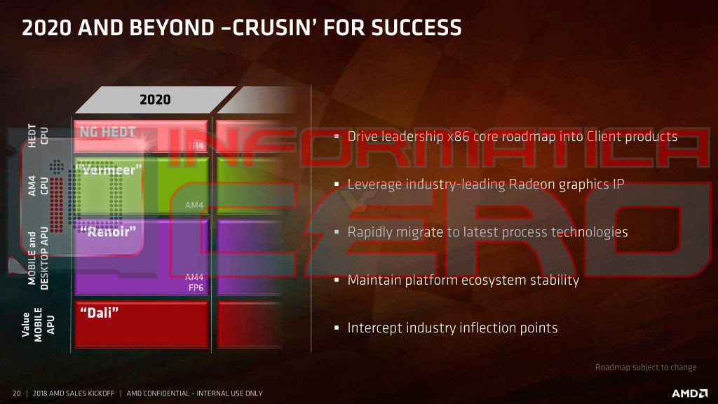
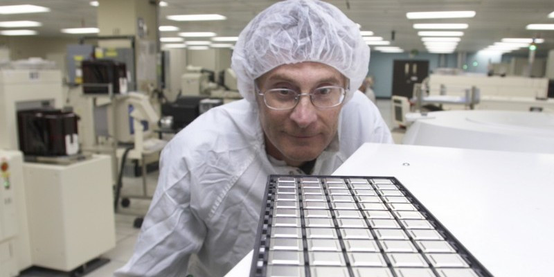
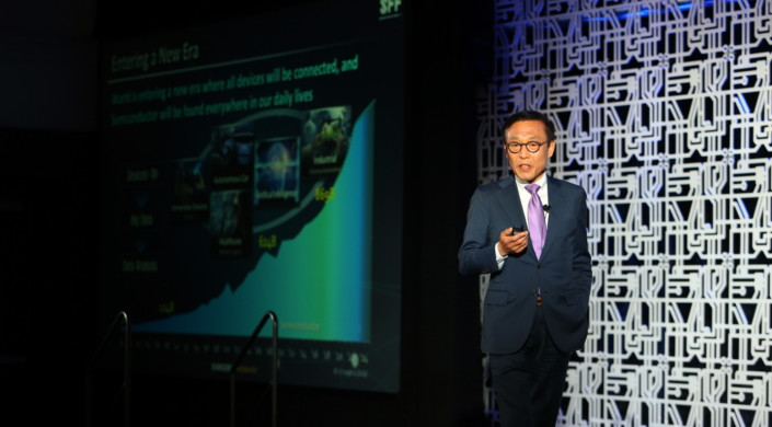
TSMC is Ramping Up 7nm Production, 5nm Next Year

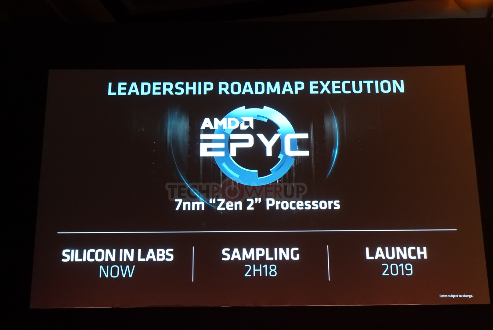
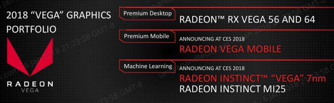
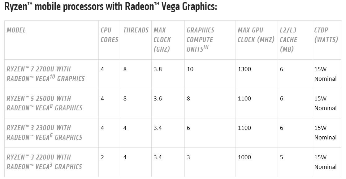
At their technology symposium in Taipei, TSMC CEO CC Wei has made remarks, dismissing speculation that their 7 nanometer yield rate was not as good as expected. Rather the company is ramping up production capacity for 7 nm quickly, up 9% from 10.5 million wafers in 2017, to 12 million wafers in 2018. They plan to tape out more than 50 chip designs in 2018, with the majority of the tape outs for AI, GPU and crypto applications, followed by 5G and application processors.

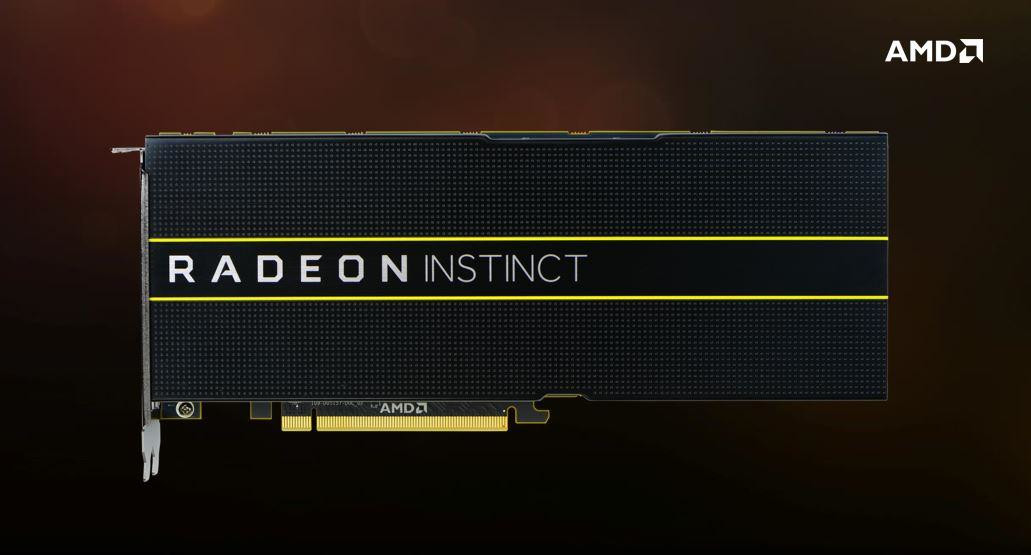
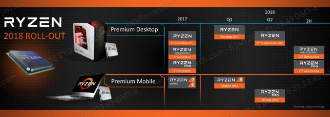
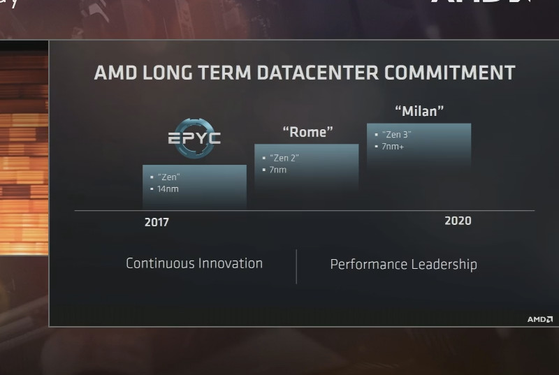
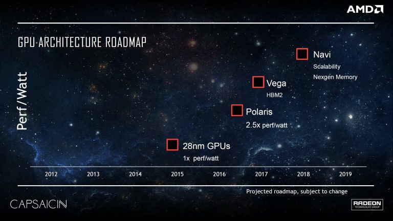
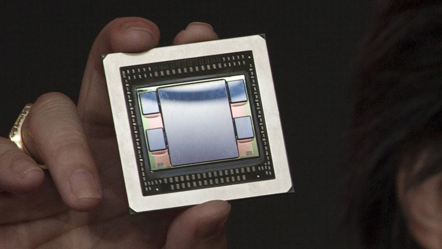
Most of their orders for the 7 nanometer node come from big players like AMD, Bitmain, NVIDIA and Qualcomm. Apple's A12 processor for upcoming iPhones is also a major driver for TSMC's 7 nanometer growth. These orders will be fulfilled in early 2019, so it'll be a bit longer before we have 7 nm processors for the masses.

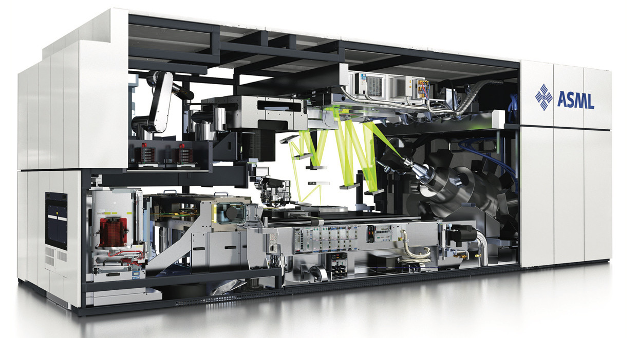
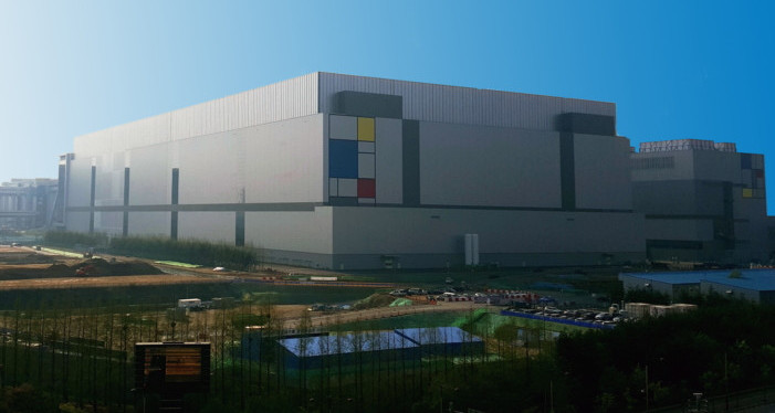
Next-gen 5 nanometer production will kick off next year, followed by mass production in late 2019 or early 2020. The company will invest as much as USD 25 billion in their new production facilities for this process node.
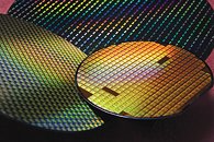
AMD to Polevault Zen+, Head Straight to 7nm Zen2 for EPYC

AMD in its Computex 2018 address earlier today, mention that its second-generation EPYC enterprise processors will be based on its 7 nanometer "Zen 2" architecture, and not 12 nm "Zen+." The company has the 7 nm silicon ready in its labs, and will begin sampling within the second half of 2018. The first products could launch in 2019, after validations. Besides improved energy-efficiency, the 12 nm "Zen+" architecture features a minor 3-5 percent IPC uplift thanks to improved multi-core clock-speed boosting, and faster caches. "Zen 2," on the other hand, presents AMD with the opportunity to make major design changes to its silicon to achieve higher IPC uplifts. The 7 nm process introduces significant transistor density uplifts over the current process. AMD is in the process of building 4-die multi-chip modules using the 12 nm "Pinnacle Ridge" silicon for its 2nd generation Ryzen Threadripper HEDT client processor family.

AMD Demonstrates 7nm Radeon Vega Instinct HPC Accelerator

AMD demonstrated the world's first GPU built on the 7 nanometer silicon fabrication process, a Radeon Vega Instinct HPC/AI accelerator, with a 7 nm GPU based on the "Vega" architecture, at its heart. This chip is an MCM of a 7 nm GPU die, and 32 GB HBM2 memory stacks over four stacks (4096-bit memory bus width). It's also the first product to feature a removable InfinityFabric interface (competition to NVIDIA's NVLink interface). There will also be variants based on the common PCI-Express 3.0 x16. The card supports hardware virtualization and new deep-learning ops.

An ARM to Rule Them All: ARM 76 To Challenge x86 Chips in the Laptop Space?

ARM has announced their next, high-performance computing solution with their A76 design, which brings another large performance increase to the fledgling architecture. having been touted for some time as a true contender to the aging x86 architecture, ARM has had a way of extracting impressive performance increases with each iteration of its computing designs, in the order of 20% do 40% performance increases in an almost annual basis. Compare that to the poster-child of x86 computing, Intel, and its passivity-fueled 5 to 10% yearly performance increases, and the projections aren't that hard to grasp: at some point in time, ARM cores will surpass x86 in performance - at least on the mobility space.

The new ARM A76 design, to be manufactured on the 7 nm process, brings about a 35% increase in performance compared to last years' A75. This comes with an added 40% power efficiency (partly from the 10 nm to 7 nm transition, the rest from architecture efficiency and performance improvements), despite the increase to maximum 3.0 GHz clocks. With the added performance, ARM is saying the new A76 will deliver 4x the Machine Learning performance of its previous A75 design.

Cadence and Micron Demo DDR5-4400 Memory Module

Cadence and Micron have joined forces to build the world's first working DDR5-4400 memory module. Cadence provided their DDR5 memory controller and PHY for the prototype while Micron produced the 8 Gb chips, which were manufactured under TSMC's 7 nm process. They were able to achieve 4400 megatransfers per second, which is roughly 37.5% faster than the fastest DDR4 memory that is currently on the market. Nevertheless, Marc Greenberg from Cadence emphasized that DDR5 aims to provide increased capacity solutions, more than actual performance.

The DDR5 standard should facilitate the production of 16 Gb dies and make vertical stacking easier. Restricted by laws of physics, dies eventually get slower as they increased in size. Once you start putting 16Gb die in 1X memory technology, the distances between them starts to get longer. As a result, core timing parameters become worse. Cadence's prototype had a CAS latency of 42 (No, not a typo). Although, the test module does run at 1.1 volts, which makes it quite impressive when compared to DDR4.

AMD to Begin Sampling 7nm "Zen 2" Processors Within 2018 for a 2019 Launch

It looks like AMD's processor product launch cycle is on steroids, and keeping up (or even ahead) of Intel. After launching the first 12 nm processor architecture with "Zen+," the company is giving final touches to what it hopes to be the world's first 7 nanometer processor architecture, with "Zen 2." The company will reportedly begin sampling the chip within 2018, to enable volume production and market launch in 2019. Speaking at an investors conference call following the company's Q1-2018 Results release, AMD CEO Dr. Lisa Su confirmed the 7 nm roll-out strategy of her company.

"We have a 7nm GPU based on Vega that we'll sample later this year. We have a 7nm server CPU that we'll sample later this year. And then, obviously, we have a number of products that are planned for 2019 as well. So it's a very, very busy product season for us. But we're pleased with the sort of the execution on the product roadmap," Dr. Su said. Unlike Zen+, Zen 2 is a major update to the company's processor micro-architecture, and presents the company with opportunities to improve several silicon-level specifications, such as the number of cores per CCX, the IPC of each core, the core-count of the die, the cache hierarchy, and the overall energy-efficiency.

AMD "Vega 20" with 32 GB HBM2 3DMark 11 Score Surfaces

With the latest Radeon Vega Instinct reveal, it's becoming increasingly clear that "Vega 20" is an optical shrink of the "Vega 10" GPU die to the new 7 nm silicon fabrication process, which could significantly lower power-draw, enabling AMD to increase clock-speeds. A prototype graphics card based on "Vega 20," armed with a whopping 32 GB of HBM2 memory, was put through 3DMark 11, on a machine powered by a Ryzen 7 1700 processor, and compared with a Radeon Vega Frontier Edition.

The prototype had lower GPU clock-speeds than the Vega Frontier Edition, at 1.00 GHz, vs. up to 1.60 GHz of the Vega Frontier Edition. Its memory, however, was clocked higher, at 1250 MHz (640 GB/s) vs. 945 MHz (483 GB/s). Despite significantly lower GPU clocks, the supposed "Vega 20" prototype appears to score higher performance clock-for-clock, but loses out on overall performance, in all tests. This could mean "Vega 20" is not just an optical-shrink of "Vega 10," but also benefits from newer architecture features, besides faster memory.

AMD Teases Its 7 nm Vega Instinct Accelerator - Data-Pushing Silicon Deployed

AMD has announced via its Twitter feed that the Vega die shrink from current 14 nm down to 7 nm has actually coalesced into a hardware product that can be tested and vetted at their labs. Via a teaser image, the company said that "7nm @RadeonInstinct product for machine learning is running in our labs."

Of course, working silicon is only half the battle - considerations such as yields, leakage, and others are all demons that must be worked out for actual production silicon, which may thus be some months off. Only AMD and TSMC themselves themselves know how the actual production run went - and the performance and power efficiency that can be expected from this design (remember that AMD's CEO Lisa SU herself said they'd partner with both TSMC and Globalfoundries for the 7 nm push, though it seems TSMC may be pulling ahead in that field). Considering AMD's timeline for the die-shrunk Vega to 7 nm - with predicted product launch for 2H 2018 - the fact that there is working silicon being sampled right now is definitely good news.

Challenges With 7 nm, 5 nm EUV Technologies Could Lead to Delays In Process' TTM

Semiconductor manufacturers have been historically bullish when it comes to the introduction of new manufacturing technologies. Intel, AMD (and then Globalfoundries), TSMC, all are companies who thrive in investors' confidence: they want to paint the prettiest picture they can in terms of advancements and research leadership, because that's what attracts investment, and increased share value, and thus, increased funds to actually reach those optimistic goals.

However, we've seen in recent years how mighty Intel itself has fallen prey to unforeseen complications when it comes to advancements of its manufacturing processes, which saw us go from a "tick-tock" cadence of new architecture - new manufacturing process, to the introduction of 14 nm ++ processes. And as Intel, Globalfoundries and TSMC race towards sub 7-nm manufacturing processes with 250 mm wafers and EUV usage, things aren't getting as rosy as the ultraviolet moniker would make us believe.

AMD "Vega 20" Optical-Shrunk GPU Surfaces in Linux Patches

AMD "Vega 20" is rumored to be an optical shrink of the current "Vega 10" GPU die to a newer process, either 12 nm, or 10 nm, or perhaps even 7 nm. Six new device IDs that point to "Vega 20" based products, surfaced on AMD's GPU drivers source code, with its latest commit made as recently as on 28th March. AMD "Vega 10" is a multi-chip module of a 14 nm GPU die, and two "10 nm-class" HBM2 memory stacks, sitting on a silicon interposer that facilitates high-density wiring between the three. In an effort to increase clock speeds, efficiency, or both, AMD could optically shrink the GPU die to a smaller silicon fabrication process, and carve out a new product line based on the resulting chip.

AMD Product Roadmap Slides for 2020 Leaked - "Castle Peak" TR4 and "Dali"

Continuing with its trend of leaking AMD slides, Spanish website Informatica Cero has now published some purported company slides leading up to AMD's 2020 strategy. New information concerns the appearance of a new, value-oriented mobile APU in the form of "Dali" - let's hope performance on that is slightly more predictable than the particular style of the artist whose name it follows. Dali therefore joins AMD's "Renoir" APU and "Vermeer" CPUs (both expected in the 7 nm process) for AMD's 2020 roadmap. This is an interesting product, which AMD is likely positioning for tablets and ultraportables.

Another interesting tidbit is AMD's outlook for their Threadripper line of HEDT CPUs. The company is looking towards its 7 nm rendition of these powerhouse chips, codenamed "Castle Peak", to bring them, in a literal way, to that figurative peak. AMD compares Threadripper to a Monster Truck of computing, and is apparently hoping to introduce Castle Peak as early as 2019. AMD then plans to further refine these "process inflection point" products in a new generation to come right after, in 2020 (much like the company has done now with Zen and Zen+).

Globalfoundries: 7 nm to Enable up to 2.7x Smaller Dies, 5 GHz CPUs

Globalfoundries' Chief Technical Officer, Gary Patton, talked about the future he believes can be possible in future manufacturing processes, calling for particular attention towards the next step in the ladder at 7 nm. Apparently, the 7 nm process at Globalfoundries has received a shot in the arm from the integration of ex IBM engineering specialists (remember that IBM practically paid Globalfoundries to take its manufacturing division of its hands), and the company now expects better than foreseen technical specs and achievements of its 7 nm process.

While a move from 14 nm to 7 nm was expected to provide, at the very best, a halving in the actual size of a chip manufactured in 7 nm compared to 14 nm, Gary Patton is now saying that the are should actually be reduced by up to 2.7 times the original size. To put that into perspective, AMD's 1000 series processors on the Zeppelin die and 14 nm process, which come in at 213 mm² for the full, 8-core design, could be brought down to just 80 mm² instead. AMD could potentially use up that extra die space to either build in some overprovisioning, should the process still be in its infancy and yields need a small boost; or cram it with double the amount of cores and other architectural improvements, and still have chips that are smaller than the original Zen dies.

Qualcomm to Build Snapdragon 5G SoCs on Samsung 7nm LPP EUV Process

Samsung Electronics, a world leader in advanced semiconductor technology, and Qualcomm Technologies, Inc., a subsidiary of Qualcomm Incorporated, today announced the intention to expand their decade-long foundry relationship into EUV (extreme ultra violet) lithography process technology, including the manufacture of future Qualcomm Snapdragon 5G mobile chipsets using Samsung's 7-nanometer (nm) LPP (Low Power Plus) EUV process technology.

Using 7LPP EUV process technology, Snapdragon 5G mobile chipsets will offer a smaller chip footprint, giving OEMs more usable space inside upcoming products to support larger batteries or slimmer designs. Process improvements, combined with a more advanced chip design, are expected to bring significant improvements in battery life.

AMD Reveals CPU, Graphics 2018-2020 Roadmap at CES

AMD at CES shed some light on its 2018 roadmap, while taking the opportunity to further shed some light on its graphics and CPU projects up to 2020. Part of their 2018 roadmap was the company's already announced, across the board price-cuts for their first generation Ryzen processors. This move aims to increase competitiveness of its CPU offerings against rival Intel - thus taking advantage of the blue giant's currently weakened position due to the exploit saga we've been covering. This move should also enable inventory clearings of first-gen Ryzen processors - soon to be supplanted by the new Zen+ 12 nm offerings, which are expected to receive a 10% boost to power efficiency from the process shrink alone, while also including some specific improvements in optimizing their performance per watt profile. These are further bound to see their market introduction in March, and are already in the process of sampling.

On the CPU side, AMD's 2018 roadmap further points towards a Threadripper and Ryzen Pro refresh in the 2H 2018, likely in the same vein as their consumer CPUs that we just talked about. On the graphics side of their 2018 roadmap, AMD focused user's attention in the introduction of premium Vega offerings in the mobile space (with HBM2 memory integration on interposer, as well), which should enable the company to compete against NVIDIA in the discrete graphics space for mobile computers. Another very interesting tidbit announced by AMD is that they would be skipping the 12 nm process for their graphics products entirely; the company announced that it will begin sampling of 7 nm Vega products to its partners, but only on the Instinct product line of machine learning accelerators. We consumers will likely have to wait a little while longer until we see some 7 nm graphics cards from AMD.

AMD Launches Ryzen APUs with Radeon Vega Graphics, Updates Roadmap

Building on the global enthusiasm generated in 2017 by Ryzen processors and Radeon graphics technology, AMD today detailed its forthcoming roll-out plan for its new and next generation of high-performance computing and graphics products during an event in Las Vegas just prior to the opening of CES 2018. Alongside announcing the first desktop Ryzen processors with built-in Radeon Vega Graphics, AMD also detailed the full line up of Ryzen mobile APUs including the new Ryzen PRO and Ryzen 3 models, and provided a first look at the performance of its upcoming 12nm 2nd generation Ryzen desktop CPU expected to launch in April. In graphics, AMD announced the expansion of the "Vega" family with Radeon Vega Mobile and that its first 7nm product is planned to be a Radeon "Vega" GPU specifically built for machine learning applications.

"We successfully accomplished the ambitious goals we set for ourselves in 2017, reestablishing AMD as a high-performance computing leader with the introduction and ramp of 10 different product families," said AMD President and CEO Dr. Lisa Su. "We are building on this momentum in 2018 as we make our strongest product portfolio of the last decade even stronger with new CPUs and GPUs that bring more features and more performance to a broad set of markets."

Rambus Talks HBM3, DDR5 in Investor Meeting

Rambus, a company that has veered around the line of being an innovative company and a patent troll, has shed some more light on what can be expected from HBM3 memory (when it's finally available). In an investor meeting, representatives from the company shared details regarding HBM3's improvements over HBM2. Details are still scarce, but at least we know Rambus' expectations for the technology: double the memory bandwidth per stack when compared to HBM2 (4000 MB/s), and a more complex design, which leaves behind the 2.5D design due to increased height of the HBM3 memory stacks. An interesting thing to note is that Rambus is counting on HBM3 to be produced on 7 nm technologies. Considering the overall semiconductor manufacturing calendar for the 7 nm process, this should place HBM3 production in 2019, at the earliest.

HBM3 is also expected to bring much lower power consumption compared to HBM2, besides increasing memory density and bandwidth. However, the "complex design architectures" in the Rambus slides should give readers pause. HBM2 production has had some apparent troubles in reaching demand levels, with suspected lower yields than expected being the most likely culprit. Knowing the trouble AMD has had in successful packaging of HBM2 memory with the silicon interposer and its own GPUs, an even more complex implementation of HBM memory in HBM3 could likely signal some more troubles in that area - maybe not just for AMD, but for any other takers of the technology. Here's hoping AMD's woes were due only to one-off snags on their packaging partners' side, and doesn't spell trouble for HBM's implementation itself.

TSMC to Build World's First 3 nm Fab in Taiwan

TSMC has announced the location for their first 3 nm fab: it will be built in the Tainan Science Park, southern Taiwan. Rumors pegged the new 3 nm factory as possibly being built in the US, due to political reasons; however, TSMC opted to keep their production capabilities clustered in the Tainan Science Park, where they can better leverage their assets and supply chain for the production and support of the world's first 3 nm semiconductor factory. It certainly also helped the Taiwanese government's decision to pledge land, water, electricity and environmental protection support to facilitate TSMC's latest manufacturing plan. It's expected that at least part of the manufacturing machines will be provided by ASML, a Netherlands-based company which has enjoyed 25% revenue growth already just this year.

As part of the announcement, TSMC hasn't given any revised timelines for their 3 nm production, which likely means the company still expects to start 3 nm production by 2022. TSMC said its 7 nm yield is ahead of schedule, and that it expects a fast ramp in 2018 - which is interesting, considering the company has announced plans to insert several extreme ultraviolet (EUV) layers at 7 nm. TSMC has also said its 5 nm roadmap is on track for a launch in the first quarter of 2019.

AMD to Build 2nd Gen. Ryzen and Radeon Vega on GloFo 12nm

Not to be held back by silicon fabrication process limitations like in the past, AMD will build its second-generation Ryzen CPUs and Radeon Vega GPUs on the new 12 nanometer LP (low power) FinFET process by GlobalFoundries. From the looks of it, "2nd generation Ryzen" doesn't seem to be the same as "Zen2" (a micro-architectural advancement due to be built on the 7 nm process), and is more likely an optical shrink of existing 14 nm IP to the 12 nm process, giving AMD the headroom to increase yields, and clock speeds across the board. The 12 nm switch allows AMD to roll out a new "generation" of Ryzen processors as early as the first half of 2018.

The "Vega 10" silicon could be another key piece of AMD IP on the receiving end of an optical shrink to 12 nm, which will give AMD much needed power savings, letting it increase clock speeds, and probably implement faster standards of HBM2 memory, such as 2.00 GT/s. AMD will likely label this shrunk down silicon "Vega 20." There's also the possibility of AMD building a bigger new GPUs altogether. In 2019, the company will give its CPU and GPU lineups major micro-architectural upgrades, and the switch to the 7 nm node. The new "Zen2" micro-architecture with IPC increases and new ISA instruction-sets, will be launched on the CPU side, and the new "Navi" graphics architecture will take center-stage.

AMD to Build "Zen 2" and "Zen 3" Processors on 7 nm Process: CTO

AMD is in no mood to stick to the 14 nm process for as long as Intel has (building four performance x86 CPU micro-architectures on it). In an interview with EE Times, AMD CTO Mark Papermaster confirmed that the company's "Zen 2" and "Zen 3" CPU micro-architectures will be built on the next-generation 7 nm silicon fab process. Transition to the 7 nm process is not as straightforward as optically shrinking your chip designs and shipping them over to your foundry. Apparently it requires big technical changes for the chip design teams, which AMD feels are better executed while it's still riding on the success of its current "Zen" architecture.

"We had to literally double our efforts across foundry and design teams…It's the toughest lift I've seen in a number of generations," said Papermaster. He added that the 7 nm node requires new "CAD tools and [changes in] the way you architect the device [and] how you connect transistors-the implementation and tools change [as well as] the IT support you need to get through it." Papermaster predicts that 7 nm will be a "long node like 28 nm" in that chip designers will have to build several refinements to their designs on the node before the newer 4 nm node could be heralded. He urged semiconductor foundry companies to introduce EUV (extreme ultra-violet lithography), a technique used to etch transistors and circuits at the infinitesimally small 7 nm node, as soon as possible, so AMD could have more options at manufacturing its next generation processors.

GLOBALFOUNDRIES on Track to Deliver Leading-Performance 7nm FinFET Technology

GLOBALFOUNDRIES today announced the availability of its 7nm Leading-Performance (7LP) FinFET semiconductor technology, delivering a 40 percent generational performance boost to meet the needs of applications such as premium mobile processors, cloud servers and networking infrastructure. Design kits are available now, and the first customer products based on 7LP are expected to launch in the first half of 2018, with volume production ramping in the second half of 2018.

In September 2016, GF announced plans to develop its own 7nm FinFET technology leveraging the company's unmatched heritage of manufacturing high-performance chips. Thanks to additional improvements at both the transistor and process levels, the 7LP technology is exceeding initial performance targets and expected to deliver greater than 40 percent more processing power and twice the area scaling than the previous 14nm FinFET technology. The technology is now ready for customer designs at the company's leading-edge Fab 8 facility in Saratoga County, N.Y.

"Our 7nm FinFET technology development is on track and we are seeing strong customer traction, with multiple product tapeouts planned in 2018," said Gregg Bartlett, senior vice president of the CMOS Business Unit at GF. "And, while driving to commercialize 7nm, we are actively developing next-generation technologies at 5nm and beyond to ensure our customers have access to a world-class roadmap at the leading edge."

IBM Research Alliance Builds New Transistor for 5 nm Technology

IBM, its Research Alliance partners GLOBALFOUNDRIES and Samsung, and equipment suppliers have developed an industry-first process to build silicon nanosheet transistors that will enable 5 nanometer (nm) chips. The details of the process will be presented at the 2017 Symposia on VLSI Technology and Circuits conference in Kyoto, Japan. In less than two years since developing a 7 nm test node chip with 20 billion transistors, scientists have paved the way for 30 billion switches on a fingernail-sized chip.

The resulting increase in performance will help accelerate cognitive computing, the Internet of Things (IoT), and other data-intensive applications delivered in the cloud. The power savings could also mean that the batteries in smartphones and other mobile products could last two to three times longer than today's devices, before needing to be charged.

Samsung Announces Comprehensive Process Roadmap Down to 4 nm

Samsung stands as a technology giant in the industry, with tendrils stretching out towards almost every conceivable area of consumer, prosumer, and professional markets. It is also one of the companies which can actually bring up the fight to Intel when it comes to semiconductor manufacturing, with some analysts predicting the South Korean will dethrone Intel as the top chipmaker in Q2 of this year. Samsung scales from hyper-scale data centers to the internet-of-things, and is set to lead the industry with 8nm, 7nm, 6nm, 5nm, 4nm and 18nm FD-SOI in its newest process technology roadmap. The new Samsung roadmap shows how committed the company is (and the industry with it) towards enabling the highest performance possible from the depleting potential of the silicon medium. The 4 nm "post FinFET" structure process is set to be in risk production by 2020.

This announcement also marks Samsung's reiteration on the usage of EUV (Extreme Ultra Violet) tech towards wafer manufacturing, a technology that has long been hailed as the savior of denser processes, but has been ultimately pushed out of market adoption due to its complexity. Kelvin Low, senior director of foundry marketing at Samsung, said that the "magic number" for productivity (as in, with a sustainable investment/return ratio) with EUV is 1,500 wafers per day. Samsung has already exceeded 1,000 wafers per day and has a high degree of confidence that 1,500 wafers per day is achievable.

AMD to Continue Working With TSMC, GLOBALFOUNDRIES on 7 nm Ryzen

In the Q&A section of their 2017 Financial Analyst Day, AMD CEO Lisa Su answered an enquiry from a Deutsche-bank questioner regarding the company's aggressive 7 nm plan for their roadmap, on which AMD seems to be balancing its process shrinkage outlook for the foreseeable future. AMD will be developing their next Zen architecture revisions on 7 nm, alongside a push for 7 nm on their next-generation (or is that next-next generation?) Navi architecture. This means al of AMD's products, consumer, enterprise, and graphics, will be eventually built on this node. This is particularly interesting considering AMD's position with GLOBALFOUNDRIES, with which AMD has already had many amendments to their Wafer Supply Agreement, a remain of AMD's silicon production division spin-off, the latest of which runs from 2016 to 2020.

As it is, AMD has to pay GLOBALFOUNDRIES for its wafer orders that go to other silicon producers (in this case, TSMC), in a quarterly basis since the beginning of 2017, based on the volume of certain wafers purchased from another wafer foundry. In addition, AMD has annual wafer purchase targets from 2016 through the end of 2020, fixed wafer prices for 2016, and a framework for yearly wafer pricing in this amendment, so the company is still bleeding money to GLOBALFOUNDRIES. However, AMD is making the correct decision in this instance, I'd wager, considering GLOBALFOUNDRIES' known difficulties in delivering their process nodes absent of quirks.

AMD to Detail Vega, Navi, Zen+ on May 16th - Laying Out a Vision

Reports are circling around the web regarding an AMD meeting featuring some of its higher ups - namely, CEO Lisa Su, head of Radeon Technologies Group Raja Koduri, and AMD's CTO Mark Papermaster happening on the 16th of May. The purpose of this meeting seems to be to discuss AMD's inflexion point, and lay out a vision for the company's future, supported on its upcoming products: the too-long-awaited Vega, its successor Navi, and the natural evolution of the company's current Zen processors, tentatively identified as Zen+.

Naturally, a company such as AMD has its roadmap planned well in advance, with work on next-generation products and technologies sometimes even running in parallel with current-generation product development. It's just a result of the kind of care, consideration, time and money that goes into making new architectures that makes this so. And while some would say Vega is now approaching a state akin to grapes that have been hanging for far too long, AMD's next graphics architecture, Navi, and its iterations on Zen cores, which the company expect to see refreshes in a 3-to-5-year period, are other matters entirely. Maybe we'll have some more details regarding the specific time of Vega's launch (for now expected on Computex), as well as on when AMD is looking to release a Zen+ refresh. I wouldn't expect much with regards to Navi - perhaps just an outline on how work is currently underway with some comments on the expectations surrounding Global Foundries' 7 nm process, on which Navi is expected to be built. And no, folks, this isn't a Vega launch. Not yet.

AMD Vega 10, Vega 20, and Vega 11 GPUs Detailed

AMD CTO, speaking at an investors event organized by Deutsche Bank, recently announced that the company's next-generation "Vega" GPUs, its first high-end parts in close to two years, will be launched in the first half of 2017. AMD is said to have made significant performance/Watt refinements with Vega, over its current "Polaris" architecture. VideoCardz posted probable specs of three parts based on the architecture.

AMD will begin the "Vega" architecture lineup with the Vega 10, an upper-performance segment part designed to disrupt NVIDIA's high-end lineup, with a performance positioning somewhere between the GP104 and GP102. This chip is expected to be endowed with 4,096 stream processors, with up to 24 TFLOP/s 16-bit (half-precision) floating point performance. It will feature 8-16 GB of HBM2 memory with up to 512 GB/s memory bandwidth. AMD is looking at typical board power (TBP) ratings around 225W.
Return to Keyword Browsing
Jul 13th, 2025 06:38 CDT change timezone

New Forum Posts

Popular Reviews

TPU on YouTube

Controversial News Posts