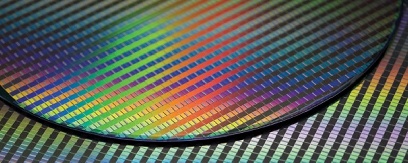
NVIDIA to Implement 7nm EUV Node for its 2020 GPUs
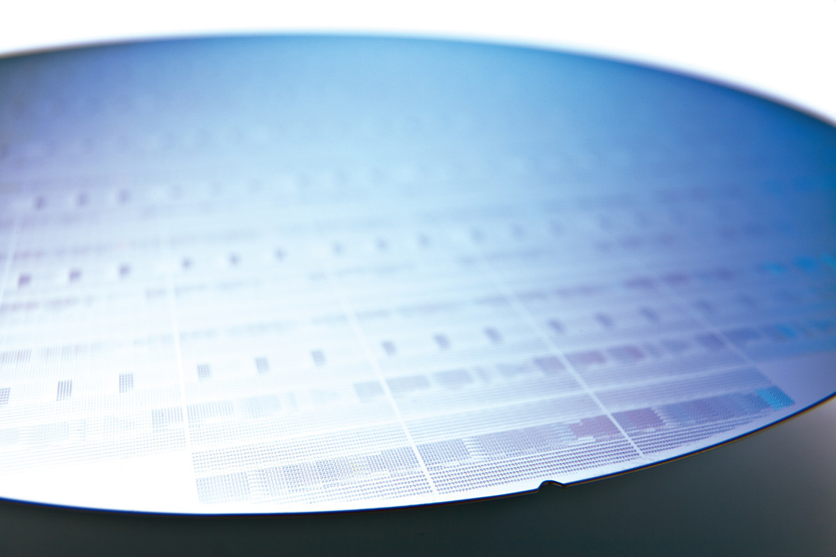
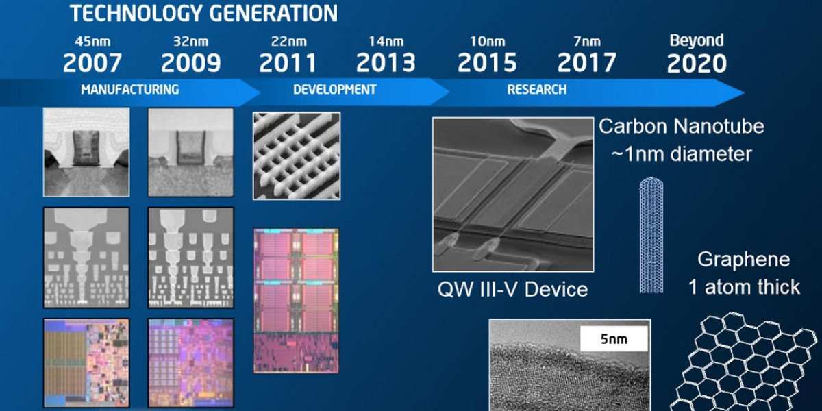
NVIDIA will implement the 7 nanometer EUV (extreme ultraviolet) lithography to build its future generation of GPUs slated for 2020, according to Japanese publication MyNavi.jp. The GPU giant could be among the first customers besides IBM, to contract Samsung for 7 nm EUV mass-production of GPUs. IBM will use the Korean semiconductor giant for manufacturing Z-series processors and FPGAs. Samsung announced in October 2018 that it will begin risk-production on its 7 nm EUV node in early-2019.
An earlier report from 2018 also forecast NVIDIA implementing 7 nm DUV (deep ultraviolet) node of TSMC for its 2019 GPU lineup. With news of the company now working with Samsung on 7 nm EUV for 2020, this seems less likely. It's possible that NVIDIA could somehow split its next generation GPU lineup between TSMC 7 nm DUV and Samsung 7 nm EUV, with the latter being used for chips with higher transistor-counts, taking advantage of the node's higher deliverable transistor densities.
An earlier report from 2018 also forecast NVIDIA implementing 7 nm DUV (deep ultraviolet) node of TSMC for its 2019 GPU lineup. With news of the company now working with Samsung on 7 nm EUV for 2020, this seems less likely. It's possible that NVIDIA could somehow split its next generation GPU lineup between TSMC 7 nm DUV and Samsung 7 nm EUV, with the latter being used for chips with higher transistor-counts, taking advantage of the node's higher deliverable transistor densities.