News Posts matching #7 nm

Return to Keyword Browsing

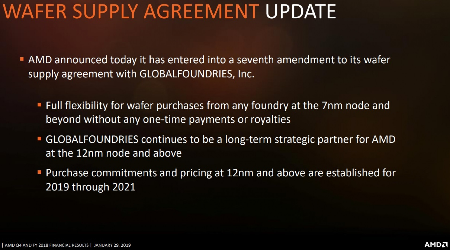
AMD to Detail Zen 2, Navi Architectures Come Hot Chips in August

The Hot Chips conference is one of the leading-edge grounds for discussion of new silicon-bound technologies, and AMD will, as usual, take to its grounds in an effort to detail their efforts in their technology fields. The conference's organization has already confirmed a number of participants in its conference schedule, which includes the likes of Intel, Microsoft, Alibaba, NVIDIA, Tesla and of course, AMD.

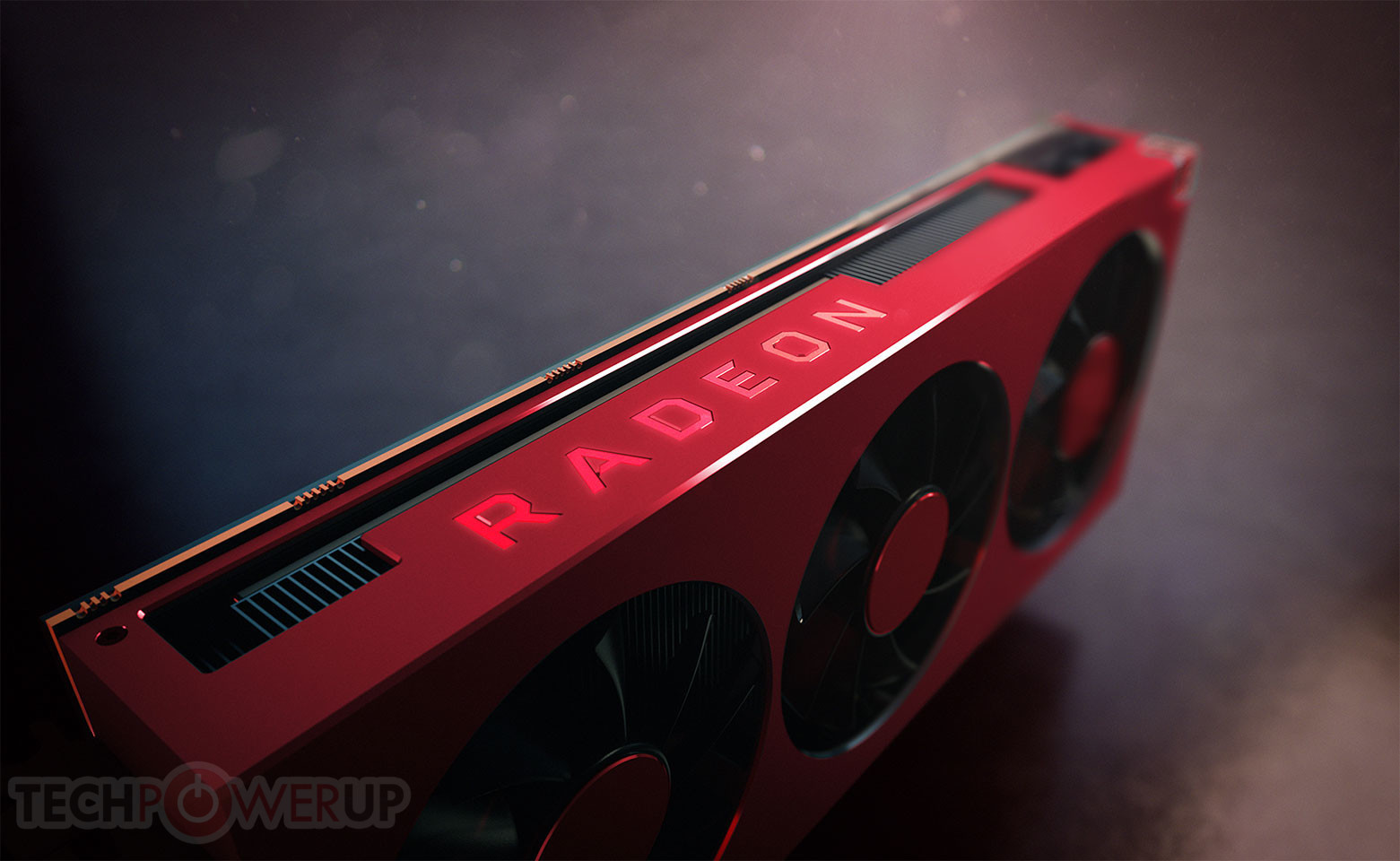
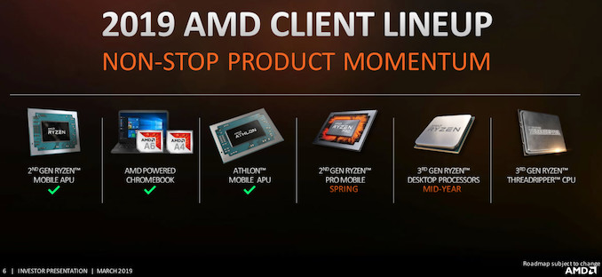
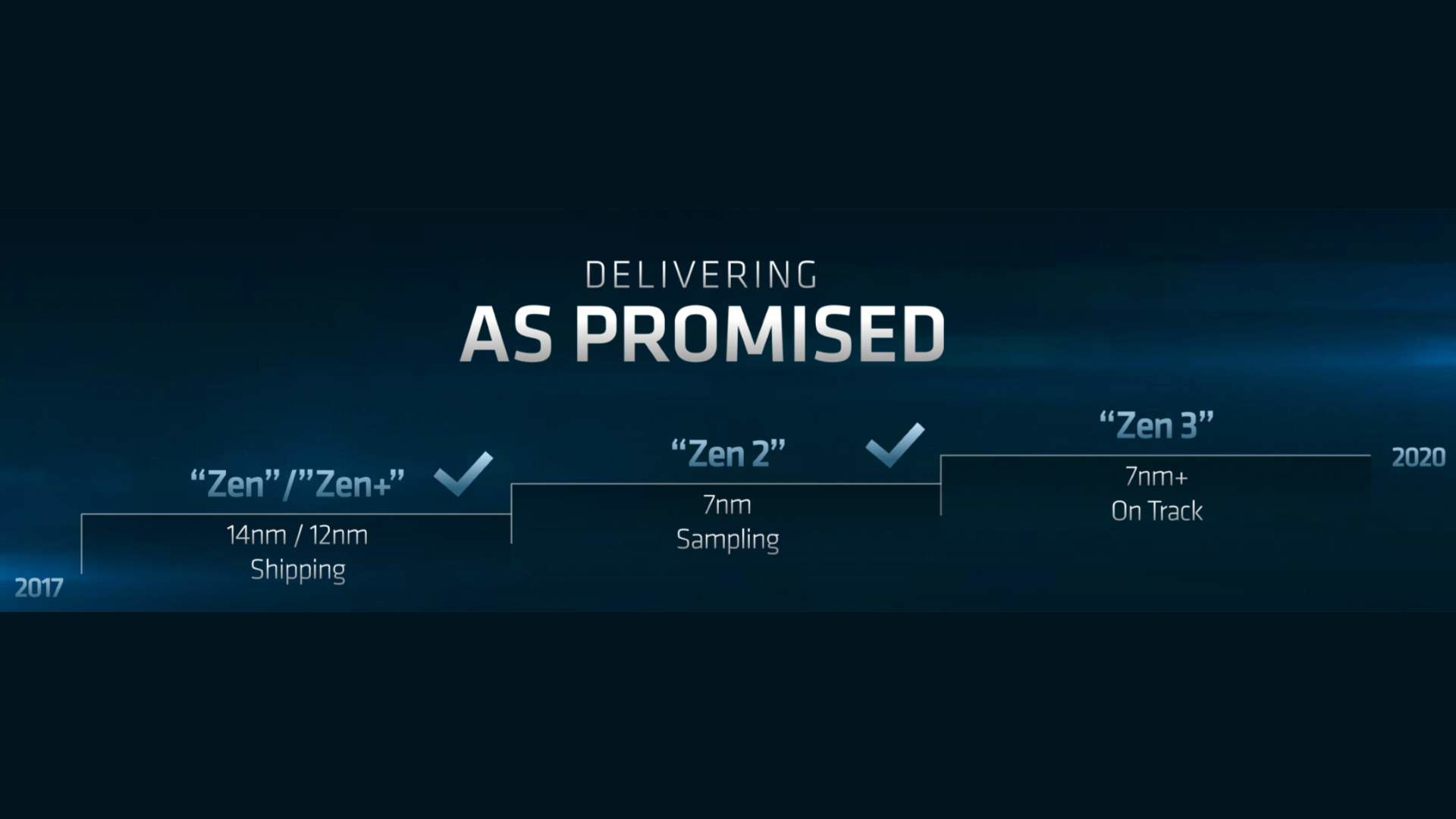
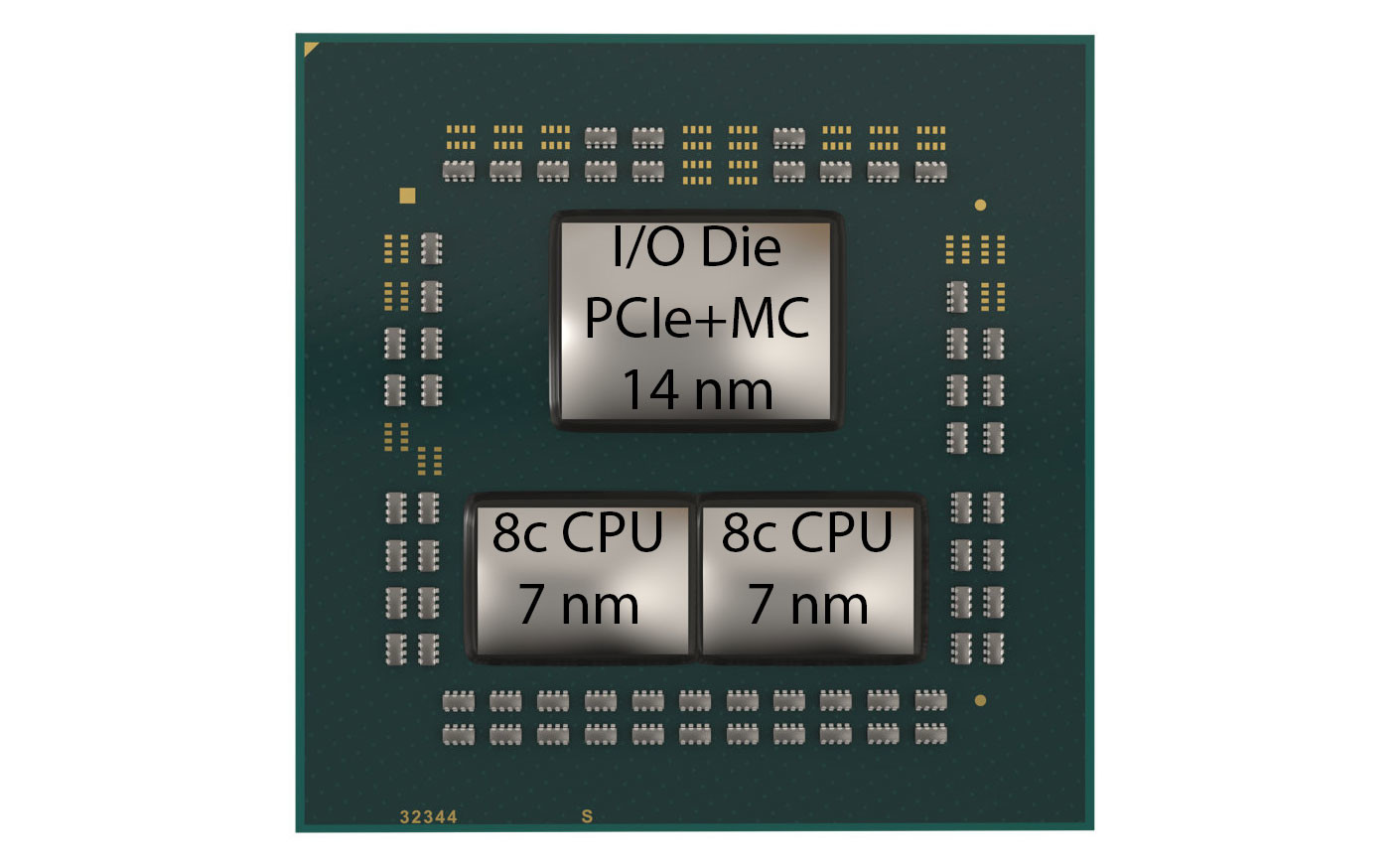
AMD will be delivering two keynotes: the first, on August 19th, is simply titled "Zen 2", and will therefore deal with the underpinnings of the Zen 2 microarchitecture, which will be pervasive to all of AMD's CPU product lines. A second conference will be held on the same day by AMD's CEO Lisa Su herself, and is titled "Delivering the Future of High-Performance Computing with System, Software and Silicon Co-Optimization". On the next day, August 20th, another AMD keynote is simply titled "7 nm Navi GPU", and we expect it to follow in the footsteps of the Zen 2 conference. So, with AMD diving deep into both architectures come August... it's extremely likely the company will have launched both product lines by then. Fingers crossed. You can find the abstract on AMD's CEO Lisa Su's conference after the break.

AMD Confirms Launch of Next-gen Ryzen, EPYC and Navi for Q3

During AMD's annual shareholder meeting today, AMD president and CEO Dr. Lisa Su confirmed the launch of next-generation AMD Ryzen, EPYC CPUs and Navi GPUs for the third quarter of this year. The expected products are going to be manufactured on TSMC's 7 nm process and will be using new and improved architectures.

Ryzen 3000 series CPUs are rumored to have up to as much as 16 cores in Ryzen 9 SKUs, 12 cores in Ryzen 7 SKUs and 8 cores in Ryzen 5 SKUs. EPYC server CPUs will be available in models up to 64 cores. All of the new CPUs will be using AMD "Zen 2" architecture that will offer better IPC performance and, as rumors suggest for consumer models, are OC beasts. Navi GPUs are the new 7 nm GPUs that are expected to be very competitive both price and performance wise to NVIDIA's Turing series, hopefully integrating new technologies such as dedicated Ray Tracing cores for higher frame rates in Ray Tracing enabled games. No next generation ThreadRipper launch date was mentioned, so we don't yet know when and if that will that land.

Intel Switches to a "Data Center First" Strategy with 7nm

Intel traditionally released new CPU microarchitectures and new silicon fabrication nodes with the client segment, and upon observing some degree of maturity with both, graduated them to the enterprise segment. With its homebrew 7 nanometer silicon fabrication process that takes flight in 2021, Intel will flip its roadmap execution strategy, by going "Data Center First." Speaking at the 2019 Investors Day summit, Intel SVP and GM of Data Center Group Navin Shenoy revealed that the first product built on Intel's 7 nm process will be a GPGPU accelerator chip derived from the Xe architecture for the Data Center, followed closely by a new server CPU. Both these products come under Shenoy's group. One is a competitor to likes of NVIDIA Tesla and AMD Radeon Instinct, while the other is a Xeon processor competing with AMD EPYC.

Shenoy explained the reason why within his group, the GPGPU product was prioritized over the server CPU. It has to do with redundancy of the GPU silicon, or specifically, the higher potential to harvest partially defective dies than CPU. A GPU has a larger number of indivisible components that can be disabled if found non-functional at the time of quality assurance, and these harvested dies can be used to carve out variants of a main product. An example of this would be NVIDIA carving out the GeForce GTX 1070 (1,920 CUDA cores) from the GP104 silicon that physically has 2,560 CUDA cores. The first manufacturing runs of the GPGPU will give the foundry valuable insights into the way the node is behaving, so it could be refined and matured for the server CPU. With 10 nm, however, Intel is sticking to the client-first model, by rolling out the "Ice Lake" processor towards the end of 2019. Within the Client Computing group, Intel has flipped its roadmap execution such that mobile (notebook) CPUs take precedence over desktop ones.

Intel Switches Gears to 7nm Post 10nm, First Node Live in 2021

Intel's semiconductor manufacturing business has had a terrible past 5 years as it struggled to execute its 10 nanometer roadmap forcing the company's processor designers to re-hash the "Skylake" microarchitecture for 5 generations of Core processors, including the upcoming "Comet Lake." Its truly next-generation microarchitecture, codenamed "Ice Lake," which features a new CPU core design called "Sunny Cove," comes out toward the end of 2019, with desktop rollouts expected 2020. It turns out that the 10 nm process it's designed for, will have a rather short reign at Intel's fabs. Speaking at an investor's summit on Wednesday, Intel put out its silicon fabrication roadmap that sees an accelerated roll-out of Intel's own 7 nm process.

When it goes live and fit for mass production some time in 2021, Intel's 7 nm process will be a staggering 3 years behind TSMC, which fired up its 7 nm node in 2018. AMD is already mass-producing CPUs and GPUs on this node. Unlike TSMC, Intel will implement EUV (extreme ultraviolet) lithography straightaway. TSMC began 7 nm with DUV (deep ultraviolet) in 2018, and its EUV node went live in March. Samsung's 7 nm EUV node went up last October. Intel's roadmap doesn't show a leap from its current 10 nm node to 7 nm EUV, though. Intel will refine the 10 nm node to squeeze out energy-efficiency, with a refreshed 10 nm+ node that goes live some time in 2020.

AMD Radeon RX 3080 XT "Navi" to Challenge RTX 2070 at $330

Rumors of AMD's next-generation performance-segment graphics card are gaining traction following a leak of what is possibly its PCB. Tweaktown put out a boatload of information of the so-called Radeon RX 3080 XT graphics card bound for an 2019 E3 launch, shortly after a Computex unveiling. Based on the 7 nm "Navi 10" GPU, the RX 3080 XT will feature 56 compute units based on the faster "Navi" architecture (3,584 stream processors), and 8 GB of GDDR6 memory across a 256-bit wide memory bus.

The source puts out two very sensational claims: one, that the RX 3080 XT performs competitively with NVIDIA's $499 GeForce RTX 2070; and two, that AMD could start a price-war against NVIDIA by aggressively pricing the card around the $330 mark, or about two-thirds the price of the RTX 2070. Even if either if not both hold true, AMD will fire up the performance-segment once again, forcing NVIDIA to revisit the RTX 2070 and RTX 2060.

AMD's Zen 2 Threadripper Conspicuously Absent From Company's Latest Roadmaps

We've all taken a look at AMD's March 2019 product roadmap, which showed us the upcoming 2019 tech the company would be bringing to the table in its "non-stop product momentum". However, it seems that this non-stop product momentum might be coming to an unexpected twist of fate that might delay it from entering the last station - the Zen 2-based Threadripper. In the company's latest May earnings call roadmap, the company silently removed the Zen 2 Threadripper from its product roadmap - where it used to sit right after the launch of Zen 2-based Ryzen products for consumers, is now just a big crop of the space it occupied.

This might mean many things, and a mistake on someone's part while cropping the PowerPoint slide could be the only thing going on here. However, the best and most plausible speculation that can be entertained when one considers this is simple - a supply problem. With the 7 nm node being the newest, most dense fabrication process possible, and with AMD having to share TSMC's 7 nm wafer production with a number of high profile companies - such as Qualcomm, for instance - may mean that supply is simply too tight to support Zen 2-based products across so many product stacks - Ryzen and Epyc - at the same time.

TSMC Expects Most 7nm Customers to Move to 6nm Density

TSMC in its quarterly earnings call expressed confidence in that most of its 7 nm (N7) process production node customers would be looking to make the transition to their 6 nm (N6) process. In fact, the company expects that node to become the biggest target for volume ordering (and thus production) amongst its customers, since the new N6 fabrication technology will bring about a sort of "backwards compatibility" with design tools and semiconductor designs that manufacturers have already invested in for its N7 node, thus allowing for cost savings for its clients.

This is despite TSMC's N6 process being able to take advantage of extreme ultraviolet lithography (EUVL) to lower manufacturing complexity. This lowering is achieved by the fact that less exposures of the silicon are required for multi-patterning - which is needed today as TSMC's N7 uses solely deep ultraviolet (DUV) lithography. Interestingly, TSMC expects other clients to pick up its N7+ manufacturing node that aren't already using their 7nm node - the need to develop new tools and lesser design compatibility between its N7 and N7+ nodes compared no N7 and N6 being the justification. TSMC's N7+ will be the first node to leverage EUV, using up to four EUVL layers, while N6 expands it up to five layers, and the upcoming N5 cranks EUVL up to fourteen (allowing for 14 layers.)

Intel Courting Samsung to Manufacture Xe GPUs?

Intel's Xe discrete GPU project head Raja Koduri recently visited a Samsung Electronics silicon fabrication facility in Korea at the backdrop of the company's major 5 nm EUV announcement. This sparks speculation that Koduri could be exploring Samsung's portfolio of sub-10 nm contract-manufacturing offerings to mass-produce Xe discrete GPUs. Intel's own foundry business is reeling with mounting pressure from the company's main breadwinner, the client and enterprise processor businesses, to get its 10 nm node on the road. Koduri's GPU would need to leverage higher transistor densities than what Intel's 10 nm could offer, given that rival AMD is already implementing 7 nm, and NVIDIA is expected to go sub-10 nm with its future generation of GPUs.

TSMC Unveils 6-nanometer Process

TSMC today announced its 6-nanometer (N6) process, which provides a significant enhancement of its industry-leading N7 technology and offers customers a highly competitive performance-to-cost advantage as well as fast time-to-market with direct migration from N7-based designs. By leveraging the new capabilities in extreme ultraviolet (EUV) lithography gained from the N7+ technology currently in risk production, TSMC's N6 process delivers 18% higher logic density over the N7 process. At the same time, its design rules are fully compatible with TSMC's proven N7 technology, allowing its comprehensive design ecosystem to be reused. As a result, it offers a seamless migration path with a fast design cycle time with very limited engineering resources for customers to achieve the product benefits from the new technology offering.

Scheduled for risk production in the first quarter of 2020, TSMC's N6 technology provides customers with additional cost-effective benefits while extending the industry-leading power and performance from the 7nm family for a broad array of applications, ranging from high-to-mid end mobile, consumer applications, AI, networking, 5G infrastructure, GPU, and high-performance computing.

AMD Zen3 to Leverage 7nm+ EUV For 20% Transistor Density Increase

AMD "Zen 3" microarchitecture could be designed for the enhanced 7 nm+ EUV (extreme ultraviolet) silicon fabrication node at TSMC, which promises a significant 20 percent increase in transistor densities compared to the 7 nm DUV (deep ultraviolet) node on which its "Zen 2" processors are being built. In addition, the node will also reduce power consumption by up to 10 percent at the same operational load. In a late-2018 interview, CTO Mark Papermaster stated AMD's design goal with "Zen 3" would be to prioritize energy-efficiency, and that it would present "modest" performance improvements (read: IPC improvements) over "Zen 2." AMD made it clear that it won't drag 7 nm DUV over more than one microarchitecture (Zen 2), and that "Zen 3" will debut in 2020 on 7 nm+ EUV.

Samsung Successfully Completes 5nm EUV Development

Samsung Electronics Co., Ltd., a world leader in advanced semiconductor technology, today announced that its 5-nanometer (nm) FinFET process technology is complete in its development and is now ready for customers' samples. By adding another cutting-edge node to its extreme ultraviolet (EUV)-based process offerings, Samsung is proving once again its leadership in the advanced foundry market.

Compared to 7 nm, Samsung's 5 nm FinFET process technology provides up to a 25 percent increase in logic area efficiency with 20 percent lower power consumption or 10 percent higher performance as a result of process improvement to enable us to have more innovative standard cell architecture. In addition to power performance area (PPA) improvements from 7 nm to 5 nm, customers can fully leverage Samsung's highly sophisticated EUV technology. Like its predecessor, 5 nm uses EUV lithography in metal layer patterning and reduces mask layers while providing better fidelity.

TSMC Completes 5 nm Design Infrastructure, Paving the Way for Silicon Advancement

TSMC announced they've completed the infrastructure design for the 5 nm process, which is the next step in silicon evolution when it comes to density and performance. TSMC's 5 nm process will leverage the company's second implementation of EUV (Extreme Ultra Violet) technology (after it's integrated in their 7 nm process first), allowing for improved yields and performance benefits.

According to TSMC, the 5 nm process will enable up to 1.8x the logic density of their 7 nm process, a 15% clock speed gain due to process improvements alone on an example Arm Cortex-A72 core, as well as SRAM and analog circuit area reduction, which means higher number of chips per wafer. The process is being geared for mobile, internet, and high performance computing applications. TSMC also provides online tools for silicon design flow scenarios that are optimized for their 5 nm process. Risk production is already ongoing.

AMD to Simultaneously Launch 3rd Gen Ryzen and Unveil Radeon "Navi" This June

TAITRA, the governing body behind the annual Computex trade-show held in Taipei each June, announced that AMD CEO Dr. Lisa Su will host a keynote address which promises to be as exciting as her CES keynote. It is revealed that Dr. Su will simultaneously launch or unveil at least four product lines. High up the agenda is AMD's highly anticipated 3rd generation Ryzen desktop processors in the socket AM4 package, based on "Zen 2" microarchitecture, and a multi-chip module (MCM) codenamed "Matisse." This launch could be followed up by a major announcement related to the company's 2nd generation EPYC enterprise processors based on the "Rome" MCM.

PC enthusiasts are in for a second major announcement, this time from RTG, with a technical reveal or unveiling of Radeon "Navi," the company's first GPU designed from the ground up for the 7 nm silicon fabrication process. It remains to be seen which market-segment AMD targets with the first "Navi" products, and the question on everyone's minds, whether AMD added DXR acceleration, could be answered. Lastly, the company could announce more variants of its Radeon Instinct DNN accelerators.

AMD President and CEO Dr. Lisa Su to Deliver COMPUTEX 2019 CEO Keynote

Taiwan External Trade Development Council (TAITRA) announced today that the 2019 COMPUTEX International Press Conference will be held with a Keynote by AMD President and CEO Dr. Lisa Su. The 2019 COMPUTEX International Press Conference & CEO Keynote is scheduled for Monday, May 27 at 10:00 AM in Room 201 of the Taipei International Convention Center (TICC) in Taipei, Taiwan with the keynote topic "The Next Generation of High-Performance Computing".

"COMPUTEX, as one of the global leading technology tradeshows, has continued to advance with the times for more than 30 years. This year, for the first time, a keynote speech will be held at the pre-show international press conference," said Mr. Walter Yeh, President & CEO, TAITRA, "Dr. Lisa Su received a special invitation to share insights about the next generation of high-performance computing. We look forward to her participation attracting more companies to participate in COMPUTEX, bringing the latest industry insights, and jointly sharing the infinite possibilities of the technology ecosystem on this global stage."

AMD Ryzen 3000 "Zen 2" BIOS Analysis Reveals New Options for Overclocking & Tweaking

AMD will launch its 3rd generation Ryzen 3000 Socket AM4 desktop processors in 2019, with a product unveiling expected mid-year, likely on the sidelines of Computex 2019. AMD is keeping its promise of making these chips backwards compatible with existing Socket AM4 motherboards. To that effect, motherboard vendors such as ASUS and MSI began rolling out BIOS updates with AGESA-Combo 0.0.7.x microcode, which adds initial support for the platform to run and validate engineering samples of the upcoming "Zen 2" chips.

At CES 2019, AMD unveiled more technical details and a prototype of a 3rd generation Ryzen socket AM4 processor. The company confirmed that it will implement a multi-chip module (MCM) design even for their mainstream-desktop processor, in which it will use one or two 7 nm "Zen 2" CPU core chiplets, which talk to a 14 nm I/O controller die over Infinity Fabric. The two biggest components of the IO die are the PCI-Express root complex, and the all-important dual-channel DDR4 memory controller. We bring you never before reported details of this memory controller.

NVIDIA GTC 2019 Kicks Off Later Today, New GPU Architecture Tease Expected

NVIDIA will kick off the 2019 GPU Technology Conference later today, at 2 PM Pacific time. The company is expected to either tease or unveil a new graphics architecture succeeding "Volta" and "Turing." Not much is known about this architecture, but it's highly likely to be NVIDIA's first to be designed for the 7 nm silicon fabrication process. This unveiling could be the earliest stage of the architecture's launch cycle, would could see market availability only by late-2019 or mid-2020, if not later, given that the company's RTX 20-series and GTX 16-series have only been unveiled recently. NVIDIA could leverage 7 nm to increase transistor densities, and bring its RTX technology to even more affordable price-points.

GlobalFoundries Looking for Buyers, Samsung and SK Hynix Seem Interested

GlobalFoundries is looking to be sold lock-stock-and-barrel by its investors, after heavily downsizing and parting with some of its Singapore-based assets recently. Once promising to lead the market with 7 nm and 5 nm advancements, the company crashed out of the sub-10 nm race, making AMD, its biggest customer, look for 7 nm supplies from TSMC. GlobalFoundries is the world's third largest semiconductor foundry service provider, with an 8.4 percent market share, behind TSMC and Samsung. Intel doesn't offer manufacturing services, as its fabs are fully dedicated to manufacturing its own products.

GlobalFoundries's main investor is Abu Dhabi-based Mubadala Technology, which holds a 90 percent stake in the company. Korean semiconductor companies Samsung and SK Hynix are reportedly in the foray to buy out GlobalFoundries, as it would give them a turnkey presence in the US, with its Upstate New York facilities. The company is unlikely to entertain bids from Chinese companies, as CFIUS would likely block the sale. "Global Foundries is unlikely to be bought by a Chinese company such as SMIC in that the U.S. government is keeping China in check in various industries," said an industry insider, adding, "The most potential candidates include South Korean companies such as Samsung Electronics and SK Hynix, and Samsung Electronics can increase its share in the market to 23 percent at once if it takes over Global Foundries."

TSMC 7nm EUV Process to Enter Mass-Production in March 2019

TSMC is giving final touches to set its flagship 7 nanometer EUV (extreme ultraviolet lithography) silicon fabrication node at its highest state of readiness for business, called mass-production. At this state, the node can mass-produce products for TSMC's customers. TSMC had taped out its first 7 nm EUV chips in October 2018. The company will also begin risk-production of the more advanced 5 nm node in April, staying on schedule. Mass production of 5 nm chips could commence in the first half of 2020.

The 7 nm EUV node augments TSMC's 7 nm DUV (deep ultraviolet lithography) node that's been already active since April 2018, and producing chips for AMD, Apple, HiSilicon, and Xilinx. At the turn of the year, 7 nm DUV made up 9 percent of TSMC's shipments. With the new node going online, 7 nm (DUV + EUV) could make up 25 percent of TSMC's output by the end of 2019.

No AMD Radeon "Navi" Before October: Report

AMD "Navi" is the company's next-generation graphics architecture succeeding "Vega" and will leverage the 7 nm silicon fabrication process. It was originally slated to launch mid-2019, with probable unveiling on the sidelines of Computex (early-June). Cowcotland reports that AMD has delayed its plans to launch "Navi" all the way to October (Q4-2019). The delay probably has something to do with AMD's 7 nm foundry allocation for the year.

AMD is now fully reliant on TSMC to execute its 7 nm product roadmap, which includes its entire 2nd generation EPYC and 3rd generation Ryzen processors based on the "Zen 2" architecture, and to a smaller extent, GPUs based on its 2nd generation "Vega" architecture, such as the recently launched Radeon VII. We expect the first "Navi" discrete GPU to be a lean, fast-moving product that succeeds "Polaris 30." In addition to 7 nm, it could incorporate faster SIMD units, higher clock-speeds, and a relatively cost-effective memory solution, such as GDDR6.

GIGABYTE Announces its Radeon VII Graphics Card

GIGABYTE, the world's leading premium gaming hardware manufacturer, today announced the launch of Radeon VII HBM2 16G, the latest Radeon VII graphics cards built upon the world's first 7nm gaming GPU. Based on the enhanced second-generation AMD 'Vega' architecture, Radeon VII is equipped with 3840 stream processors and 16GB of ultra-fast HBM2 memory (second-generation High-Bandwidth Memory). It is designed to deliver exceptional performance and amazing experiences for the latest AAA, e-sports and Virtual Reality (VR) titles, demanding 3D rendering and video editing applications, and next-generation compute workloads.

According to the AMD official website, the Radeon VII graphics card enables high-performance gaming and ultra-high quality visuals. Ground-breaking 1 TB/s memory bandwidth and a 4,096-bit memory interface paves the way for ultra-high resolution textures, hyper-realistic settings and life-like characters. With the high speeds of today's graphics cards, framerates often exceed the monitor refresh rate, causing stuttering and tearing.

AMD Updates Wafer Supply Agreement with GlobalFoundries to Free Itself of "7nm Tax"

AMD in its Q4-2018 Earnings Report disclosed that it has amended its Wafer Supply Agreement (WSA) with GlobalFoundries that frees it from paying a "7 nanometer tax." Under the older version of WSA, AMD would have had to pay a penalty to GlobalFoundries if it sourced processors from any other semiconductor foundry. The company got preferential pricing in return for the exclusivity. With GlobalFoundries discontinuing development of cutting-edge processes such as 7 nm and 5 nm, it makes sense for AMD to seek out other foundry partners, such as TSMC, and an amendment to the WSA was needed. With this amendment in place, AMD can go ahead and source 7 nm dies from TSMC without paying penalties to GlobalFoundries (GloFo).

With its "Zen 2" microarchitecture, AMD is going big on multi-chip modules, in which only those components that can tangibly benefit from the switch to the 7 nm node, namely the CPU cores, would be built on 7 nm dies, called "CPU chiplets," while components that don't need the miniaturization just yet, such as the processor's memory controller, PCIe root-complex, etc., will be built on separate dies called "I/O controllers." These dies will continue to be 14 nm, and likely supplied by GloFo. Final packaging of 7 nm CPU chiplets from TSMC, and 14 nm I/O controllers from GloFo, will happen at GloFo's facilities in China or Malaysia. AMD in its amendment committed to purchasing 14 nm and 12 nm chips from GloFo between 2019 and 2021, which means the MCM approach to processors is here to stay.

TSMC's 7 nm Fabrication Becomes Biggest Share of Revenue in 4Q18

TSMC's introduction of its 7 nm fabrication technology has essentially propelled the company to silicon manufacturing heights. Every company - particularly in the mobile space - is after the most minute increase in transistor density and power consumption improvements the latest and greatest can bring. AMD themselves have become a major TSMC partner in pursuit of its newfound competitiveness against Intel, and has apparently leveraged the 7 nm process as a way to keep its high-performance GPU offering minimally competitive with NVIDIA's solution - at a much lesser die area requirement, if the Radeon VII vs RTX 2080 estimates are something to go by.

As a consequence of the market interest for the 7 nm process, it has rapidly become TSMC's biggest revenue generator as soon as 4Q18. The company said that 7 nm already generated 10% of the company's entire 2018 revenue, despite the process only having been ramped up in June of the same year. Other less dense technologies still generate a lot of revenue for the company, and are likely much higher volume. However, TSMC is most likely riding on much increased ASP for 7 nm wafers than for other technologies.

A Sprinkle of Salt: AMD Radeon VII Reported to Only be Available in Reference Design, no Custom Treatment

A report via Tom's Hardware.de says that AMD's plans for the upcoming Radeon VII are somewhat one-dimensional, in that only reference designs will be available for this particular rendition of the Vega architecture. And this doesn't mean"initial availability" only on reference cards, like NVIDIA has been doing with their Founder's editions; the report claims that at no point in time will there actually be a custom-designed Radeon VII. The quantity of Radeon VII GPUs will apparently be "strictly limited" come launch - a likely result of the decision to make use of TSMC's 7 nm process, which will have to serve not only AMD's Ryzen 3000 and Epyc CPUs when those are actually launched, but all of TSMC's other clients.

This is in contrast with AMD CEO Lisa Su's words during her CES keynote, who said that Radeon VII would be available from "several leading add-in board partners plan to offer the cards". According to a Tom's Hardware.de Taiwanese source, "You cannot leak anything that does not exist" in regards to third-party designs. And another Chinese source said "the quantity of Radeon VII is strictly limited… not sure if AMD wants to open AIB to have an own design later".

AMD CTO Mark Papermaster Confirms 7 nm Lineup Refresh for 2019

AMD's CTO Mark Papermaster, in an interview with TheStreet, confirmed AMD's plans with 7 nm for their graphics offerings are just beginning with Radeon VII. When inquired on AMD's plans for their graphics division, Papermaster said that "What we do over the course of the year is what we do every year. We'll round out the whole roadmap." he then added that "We're really excited to start on the high-end... you'll see the announcements over the course of the year as we round out our Radeon roadmap."

So these comments form papermaster seemingly confirm two things: first, that AMD plans to "round out" its lineup using the 7 nm process technology, which means increasing offerings at different price points. The use of the word "refresh" almost takes the breath away, since refreshes are usually based on the same previous architectures. However, AMD does have plans for a new mid-range chip to finally succeed Polaris in Navi, which should become the next AMD launch in the 7 nm process for graphics technologies.

AMD Radeon VII Detailed Some More: Die-size, Secret-sauce, Ray-tracing, and More

AMD pulled off a surprise at its CES 2019 keynote address, with the announcement of the Radeon VII client-segment graphics card targeted at gamers. We went hands-on with the card earlier this week. The company revealed a few more technical details of the card in its press-deck for the card. To begin with, the company talks about the immediate dividends of switching from 14 nm to 7 nm, with a reduction in die-size from 495 mm² on the "Vega 10" silicon to 331 mm² on the new "Vega 20" silicon. The company has reworked the die to feature a 4096-bit wide HBM2 memory interface, the "Vega 20" MCM now features four 32 Gbit HBM2 memory stacks, which make up the card's 16 GB of memory. The memory clock has been dialed up to 1000 MHz from 945 MHz on the RX Vega 64, which when coupled with the doubled bus-width, works out to a phenomenal 1 TB/s memory bandwidth.

We know from AMD's late-2018 announcement of the Radeon Instinct MI60 machine-learning accelerator based on the same silicon that "Vega 20" features a total of 64 NGCUs (next-generation compute units). To carve out the Radeon VII, AMD disabled 4 of these, resulting in an NGCU count of 60, which is halfway between the RX Vega 56 and RX Vega 64, resulting in a stream-processor count of 3,840. The reduced NGCU count could help AMD harvest the TSMC-built 7 nm GPU die better. AMD is attempting to make up the vast 44 percent performance gap between the RX Vega 64 and the GeForce RTX 2080 with a combination of factors.
Return to Keyword Browsing
Jul 14th, 2025 19:06 CDT change timezone

New Forum Posts

Popular Reviews

TPU on YouTube

Controversial News Posts