News Posts matching #7 nm

Return to Keyword Browsing

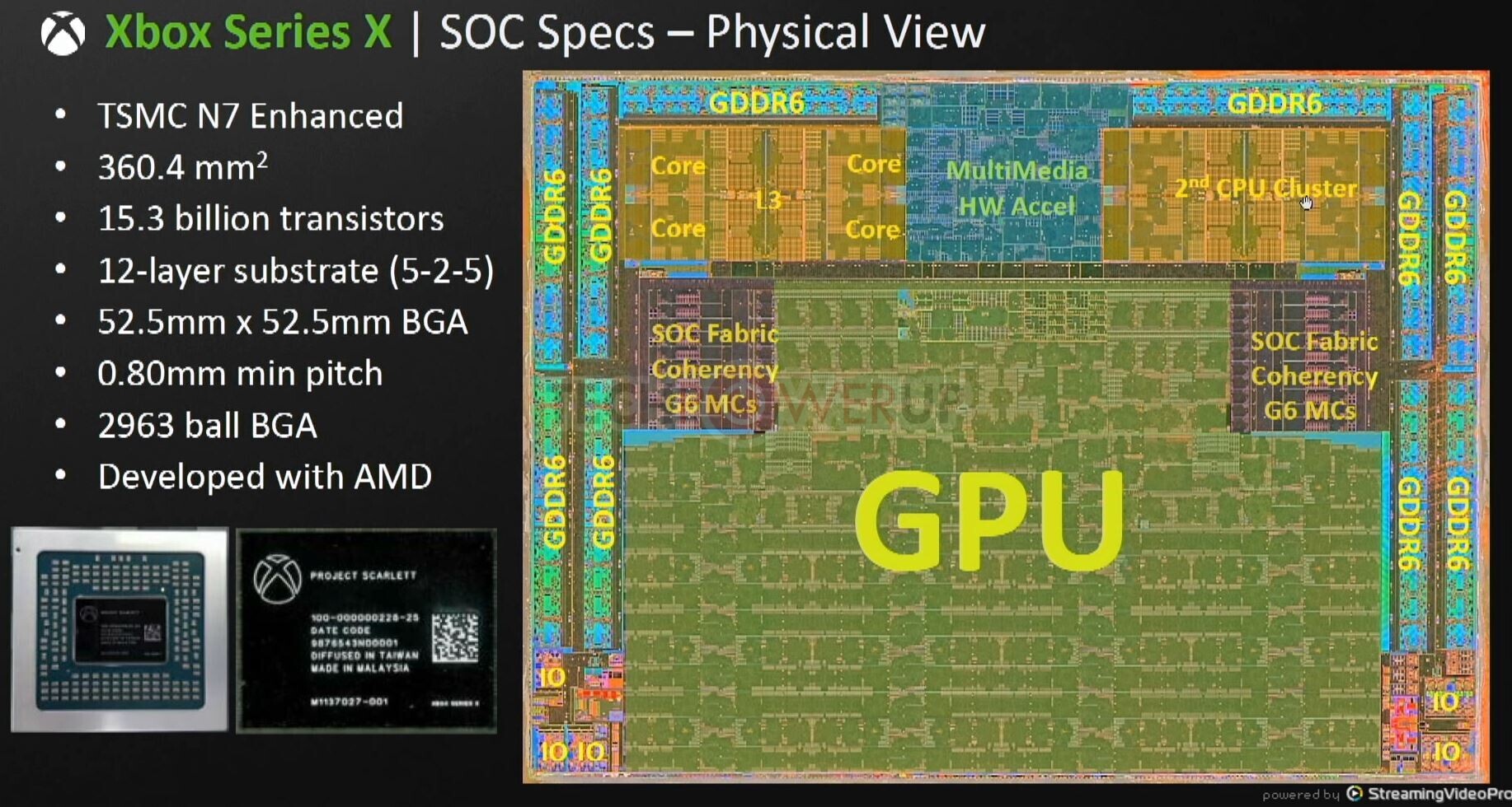
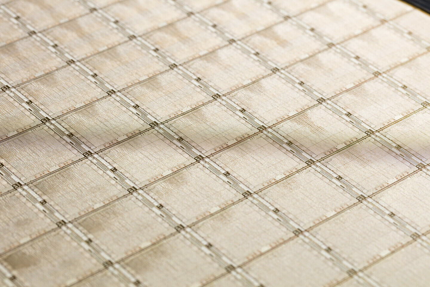
Raja Koduri to Present at Samsung Foundry Forum amid Intel's Outsourcing Efforts

Intel's chief architect and senior vice president of discrete graphics division, Mr. Raja Koduri, is said to be scheduled to present at Samsung Electronics Event day. With a presentation titled "1000X More Compute for AI by 2025", the event is called Samsung Foundry SAFE Forum. It is a global virtual conference designed to be available to everyone. So you might be wondering what is Mr. Koduri doing there. Unless you have been living under a rock, you know about Intel's struggles with node manufacturing. Specifically, the 10 nm node delays that show the company's efforts to deliver a node on time. The same is happening with the 7 nm node that also experienced significant delays.

Intel has a contract to develop an exascale supercomputer at Argonne National Laboratory, called Aurora. That supercomputer is using Intel's CPUs and the company's upcoming Xe GPUs. Since the company has problems with manufacturing and has to deliver the products (it is bound by several contracts) to its contractors and customers, it decided to look at external manufacturers for its products, specifically Xe graphics. Being that Mr. Koduri tweeted an image of him visiting Samsung Giheung Fab in Korea, and now presenting at the Samsung Foundry event, it is possible that Intel will tap Samsung's semiconductor manufacturing process for its Xe GPU efforts and that Samsung will be the contractor in charge.

AMD Radeon RX 6000 Series Specs Leak: RX 6900 XT, RX 6800 XT, RX 6700 Series

AMD's Radeon RX 6000 series graphics cards, based on the RDNA2 graphics architecture, will see the introduction of the company's first DirectX 12 Ultimate graphics cards (featuring features such as real-time raytracing). A VideoCardz report sheds light on the specifications. The 7 nm "Navi 21" and "Navi 22" chips will power the top-end of the lineup. The flagship part is the Radeon RX 6900 XT, followed by the RX 6800 XT and RX 6800; which are all based on the "Navi 21." These are followed by the RX 6700 XT and RX 6700, which are based on the "Navi 22" silicon.

The "Navi 21" silicon physically features 80 RDNA2 compute units, working out to 5,120 stream processors. The RX 6900 XT maxes the chip out, enabling all 80 CUs, and is internally referred to as the "Navi 21 XTX." Besides these, the RX 6900 XT features 16 GB of GDDR6 memory across a 256-bit wide memory interface, and engine clocks boosting beyond 2.30 GHz. The next SKU in AMD's product stack is the RX 6800 XT (Navi 21 XT), featuring 72 out of 80 CUs, working out to 4,608 stream processors, the same 16 GB 256-bit GDDR6 memory configuration as the flagship, while its engine clocks go up to 2.25 GHz.

China's SMIC Announces N+1 Node Tape-Out for 7 nm Silicon

SMIC is taking immense strides in bridging the gap between China's in-house silicon manufacturing capability compared to the usual Taiwanese or US-based options. Despite its ties to the Chinese government, which led for a US blacklisting of the company amidst the current China-US trade-war, SMIC has definitely achieved a benchmark with its 7 nm tape-out. This was achieved after a number of funding rounds, some of them with the power of the Chinese state behind them. While the blacklisting definitely hurt the company, they still have access to ASML's semiconductor manufacturing equipment, so while the rope may be tight, it likely isn't suffocating.

The node's first production tape-out is for an ASIC (Application-Specific Integrated Circuit) design for Innosilicon, which specializes in cryptocurrency mining, purpose-built chips. SMIC states that the new N+1 process can offer up to 20% boosted performance at the same clocks and core complexity compared to their 12 nm designs, which is subpar compared to other player's "7 nm class nodes", such as GloFo's 12 LP+, Samsung's 8LPP and TSMC's N7 non-EUV nodes (TSMC, for instance, offered a 20% performance boost between the 10 nm and 7 nm nodes). SMIC's manufacturing looks better in other metrics, though: power requirements can be reduced by 57% at the same TDP and complexity, and the transistor density can be increased by up to 2.7 times, (the "up to" depends on specific semiconductor structures). This is SMIC is only targeting - for now - low-power and low-cost devices with the N+1 nodes.

NVIDIA Reportedly Moving Ampere to 7 nm TSMC in 2021

A report straight from DigiTimes claims that NVIDIA is looking to upgrade their Ampere consumer GPUs from Samsung's 8 nm to TSMC's 7 nm. According to the source, the volume of this transition should be "very large", but most likely wouldn't reflect the entirety of Ampere's consumer-facing product stack. The report claims that TSMC has become more "friendly" to NVIDIA. This could be because TSMC now has available manufacturing capacity in 7 nm due to some of its clients moving to the company's 5 nm node, or simply because TSMC hadn't believed NVIDIA to consider Samsung as a viable foundry alternative - which it now does - and has thus lowered pricing.

There are various reasons being leveraged at this, none with substantial grounds other than "reported from industry sources". NVIDIA looking for better yields is one of the appointed reasons, as is its history as a TSMC customer. NVIDIA shouldn't have too high a cost porting its manufacturing to TSMC in terms of design changes to the silicon level so as to cater to different characteristics of TSMC's 7 nm, because the company's GA100 GPU (Ampere for the non-consumer market) is already manufactured at TSMC. The next part of this post is mere (relatively informed) speculation, so take that with a saltier disposition than what came before.

AMD Ryzen 5000 "Zen 3" "Vermeer" Launch Liveblog

AMD is announcing its next-generation Ryzen 5000 series desktop processors in the Socket AM4 package. These 7 nm processors see the implementation of the company's new "Zen 3" microarchitecture, and are expected to push the performance envelope. AMD CEO Dr Lisa Su takes centerstage in a pre-recorded launch event stream which we are live-blogging. These are facts as they appear, along with our analysis.

Update 16:01 UTC: Looks like this is a pre-recorded stream made to look live (a premiere).

Intel Starts Hardware Enablement of Meteor Lake 7 nm Architecture

In a report by Phoronix, we have the latest information about Intel's efforts to prepare the next generation of hardware for launch sometime in the future. In the latest Linux kernel patches prepared to go mainline soon, Intel has been adding support for its "Meteor Lake" processor architecture manufactured on Intel's most advanced 7 nm node. While there are no official patches in the mainline kernel yet, the first signs of Meteor Lake are expected to show up in the version 5.10, where we will be seeing the mentions of it. This way Intel is ensuring that the Meteor Lake platform will see the best software support, even though it is a few years away from the launch.

Meteor Lake is expected to debut in late 2022 or 2023, which will replace the Alder Lake platform coming soon. In a similar way to Alder Lake, Meteor Lake will use a hybrid core technology where it will combine small and big cores. The Meteor Lake platform will use the new big "Ocean Cove" design paired with small "Gracemont" cores that will be powering the CPU. This processor is going to be manufactured on Intel's 7 nm node that will be the first 7 nm design from Intel. With all the delays to the node, we are in for an interesting period to see how the company copes with it and how the design IPs turn out.

First Signs of AMD Zen 3 "Vermeer" CPUs Surface, Ryzen 7 5800X Tested

AMD is preparing to launch the new iteration of desktop CPUs based on the latest Zen 3 core, codenamed Vermeer. On October 8th, AMD will hold the presentation and again deliver the latest technological advancements to its desktop platform. The latest generation of CPUs will be branded as a part of 5000 series, bypassing the 4000 series naming scheme which should follow, given that the prior generation was labeled as 3000 series of processors. Nonetheless, AMD is going to bring a new Zen 3 core with its processors, which should bring modest IPC gains. It will be manufactured on TSMC's 7 nm+ manufacturing node, which offers a further improvement to power efficiency and transistor density.

Today, we have gotten the first benchmark of AMD's upcoming Ryzen 7 5800X CPU. Thanks to the popular hardware leaker, TUP APISAK, we have the first benchmark of the new Vermeer processor, compared to Intel's latest and greatest - Core i9-10900K. The AMD processor is an eight-core, sixteen threaded model compared to the 10C/20T Intel processor. While we do not know the final clocks of the AMD CPU, we could assume that the engineering sample was used and we could see an even higher performance. Below you can see the performance of the CPU and how it compares to Intel. By the numbers shown, we can expect AMD to possibly be a new gaming king, as the numbers are very close to Intel. The average batch result for the Ryzen 7 5800X was 59.3 FPS and when it comes to CPU frames it managed to score 133.6 FPS. Intel's best managed to average 60.3 FPS and 114.8 FPS from the CPU framerates. Both systems were tested with NVIDIA's GeForce RTX 2080 GPUs.

Intel 14 nm Node Compared to TSMC's 7 nm Node Using Scanning Electron Microscope

Currently, Intel's best silicon manufacturing process available to desktop users is their 14 nm node, specifically the 14 nm+++ variant, which features several enhancements so it can achieve a higher frequencies and allow for faster gate switching. Compare that to AMD's best, a Ryzen 3000 series processor based on Zen 2 architecture, which is built on TSMC's 7 nm node, and you would think AMD is in clear advantage there. Well, it only sort of is. German hardware overclocker and hacker, der8auer, has decided to see how one production level silicon compares to another, and he put it to the test. He decided to use Intel's Core i9-10900K processor and compare it to AMD's Ryzen 9 3950X under a scanning electron microscope (SEM).

First, der8auer took both chips and detached them from their packages; then he proceeded to grind them as much as possible so SEM could do its job of imaging the chips sans the substrate and protective barrier. This was followed by securing the chips to a sample holder using an electrically conductive adhesive to improve penetration of the high energy electrons from the SEM electron gun. To get as fair a comparison as possible, he used the L2 cache component of both processors as they are usually the best representatives of a node. This happens because the logic portion of the chip differs according to architecture; hence, level two cache is used to get a fair comparison - it's design is much more standardized.

AMD "Vermeer" Zen 3 Processors Branded Under Ryzen 5000 Series?

AMD is allegedly preparing to market its next-generation Socket AM4 desktop processors based on the "Vermeer" MCM, under the Ryzen 5000 Series. The "Vermeer" MCM implements the company's "Zen 3" microarchitecture in the client segment. It features up to two 7 nm-class CPU complex dies with up to 8 cores, each, and a refreshed cIOD (client IO die). AMD has allegedly improved the cIOD with a new memory controller and several new toggles that improve memory bandwidth. The cIOD combines a PCI-Express Gen 4 root complex with a dual-channel DDR4 memory controller. With "Zen 3," AMD is also introducing an improved boosting algorithm, and an improved SMT feature.

Coming back to AMD's rumored nomenclature, and we could see the company bumping up its processor model numbers to the 5000 series for equivalent core-counts. For example, the Ryzen 9 5900X is a 12-core/24-thread part, much like the 3900X; whereas the Ryzen 7 5800X is an 8-core/16-thread part. This flies in the face of rumors that AMD could take advantage of the 8-core CCX design of the "Zen 3" microarchitecture by carving out 10-core parts using two CCDs with 5 cores enabled, each. The reason AMD is skipping the 4000 series numbering with "Vermeer" probably has something to do with "Renoir" taking up many of the 4000-series model numbers. "Renoir" is based on "Zen 2," and recently made its desktop debut, albeit as an OEM-exclusive. The company is planning to introduce certain 4000G series models to the DIY retail segment. AMD is expected to announce its first "Zen 3" client-segment processors on October 8, 2020.

Alleged Prices of TSMC Silicon Wafers Appear

TSMC, one of the biggest silicon manufacturers in the world, usually doesn't disclose company pricing of the silicon it manufactures and only shares that with its customers. It appears that RetiredEngineer (@chiakokhua on Twitter) got a hold of the pricing of TSMCs wafers on every manufacturing node starting from 90 nm down to 5 nm. That includes a wide portfolio of 65, 40, 28, 20, 16/12, 10, and 7 nm nodes as well. The table shown below includes information dating to April 2020, so it is possible that some things are now different and they surely are. There are a few quite interesting notes from the image, namely the price increase as the node shrinks.

From 90 nm to 20 nm, the price of the wafer didn't increase as much, however, starting from 16/12 nm node(s), TSMC has seen costs per wafer, and other costs increase exponentially. For example, just compare the 10 nm wafer price of $5992 with the price of a 5 nm wafer which costs an amazing $16988. This is more than a 180% price increase in just three years, however, the cost per transistor is down as you get around 229% higher density in that period, making TSMC actually in line with Moore's Law. That is comparing Transistor density (MTr / mm²) of52.51 million transistors for the 10 nm node and 173 million transistors per mm² of the 5 nm node .

PlayStation 5 Launch Supply Reduced due to AMD CPU/GPU SoC Yield Issues

Today we have found out that Sony has reportedly cut PlayStation 5 launch supply due to bad yields of the SoC powering the console. Previously, we reported that Sony has doubled production of the new console amid high demand, where the company expected to sell 10 million units in the fiscal year. The original plan was to have around 15 million units of the new console available by March 31st, 2021. Sony has been spending a lot of resources to get as many units out to consumers, however, the bad SoC yields have held the company back significantly.

It is reported by Bloomberg that instead of the original 15 million units Sony plans to supply, there will be only 11 million of them. That represents a massive reduction of 4 million units. And you are wondering how bad the yields of the new SoC are to have that big reduction. According to the source, TSMC and Sony are seeing only 50% yields on the production run. It is reported that the yields are gradually improving but have not yet reached the level needed to have a stable supply. This represents a big problem for the company and we don't know who is to blame. TSMC has been very good at manufacturing 7 nm silicon, however, it could be bad design from AMD and Sony that is making the production difficult. We are waiting for more information.

MSI Announces Alpha 15 & 17 Models Powered by AMD Ryzen 7 4800H + Radeon RX 5600M

As digital games are quickly emerging as one of the world's favorite pastimes, gaming laptop giant MSI continues to produce innovative laptops to meet the diverse demands of gamers. MSI's all-AMD laptops, Alpha 15 and 17, are making a strong comeback with more powerful specifications, offering the latest 7 nm-powered AMD mobile processor and graphics technology.

Designed for gamers looking for the most advanced technology, MSI's all-AMD Alpha 15 and 17 gaming laptops combine the cutting-edge hardware of up to AMD Ryzen 7 4800H mobile processor and AMD Radeon RX 5600M graphics, which together offer desktop-class performance as an appealing and affordable option for mainstream gamers. As the chart indicates, the 7 nm combination significantly expedites the speed and performance for multitasking, heavy workloads, or playing popular games like "Grand Theft Auto V", "Shadow of the Tomb Raider" and "Borderlands 3".

MediaTek Advances its 5G Platform with New T750 5G Chipset for Routers and Hotspots

MediaTek today announced its T750 5G chipset to power next generation 5G CPE wireless products, like fixed wireless access routers (FWA) and mobile hotspots, to bring fast 5G connectivity into homes, businesses and anyone on the go. The highly integrated, 7 nm compact chip design comes with an integrated 5G radio and quad-core Arm CPU. It's full-featured with all the essential functions and peripherals for device makers to build high performance consumer premise equipment products in the smallest form factors possible. The T750 is sampling now with potential customers.

"Pervasive high-speed broadband connectivity is becoming more important with the increase in connected devices and the surge of people working from home, taking online classes and using services like tele-health and video calling," said JC Hsu, Corporate Vice President and General Manager of MediaTek's wireless communications business unit. "We are extending our 5G leadership beyond the smartphone segment with the T750 chipset, opening up new markets for broadband operators and device makers, and helping consumers - no matter where they live - to experience all the advantages of 5G connectivity."

AMD Rolls Out Radeon RX 5300: 1408 SP, 3GB GDDR6

AMD sneaked out the Radeon RX 5300 desktop discrete graphics card. At this point it's unclear if the card is an OEM exclusive, or if a retail channel launch is imminent. The RX 5300 desktop features an identical core-configuration to the RX 5300M mobile GPU that's been out since late-2019. The desktop RX 5300 surfaced on the Geekbench database in May 2020.

Based on the 7 nm "Navi 14" silicon, the RX 5300 is endowed with the same 1,408 stream processor count as the RX 5500 XT, but the memory amount and bus width has been cut down by 25%. It hence has 3 GB of GDDR6 memory across a 96-bit wide memory interface, which at 14 Gbps puts out 168 GB/s of memory bandwidth. The GPU ticks at 1448 MHz "game" clocks, and 1645 MHz boost. The typical board power of the RX 5300 is rated at 100 W, which means it requires at least a 6-pin PCIe power input and cannot make do with slot-only power. There's no word on pricing, since we have no info on channel-based availability.

NVIDIA GeForce RTX 3090 and 3080 Specifications Leaked

Just ahead of the September launch, specifications of NVIDIA's upcoming RTX Ampere lineup have been leaked by industry sources over at VideoCardz. According to the website, three alleged GeForce SKUs are being launched in September - RTX 3090, RTX 3080, and RTX 3070. The new lineup features major improvements: 2nd generation ray-tracing cores and 3rd generation tensor cores made for AI and ML. When it comes to connectivity and I/O, the new cards use the PCIe 4.0 interface and have support for the latest display outputs like HDMI 2.1 and DisplayPort 1.4a.

The GeForce RTX 3090 comes with 24 GB of GDDR6X memory running on a 384-bit bus at 19.5 Gbps. This gives a memory bandwidth capacity of 936 GB/s. The card features the GA102-300 GPU with 5,248 CUDA cores running at 1695 MHz, and is rated for 350 W TGP (board power). While the Founders Edition cards will use NVIDIA's new 12-pin power connector, non-Founders Edition cards, from board partners like ASUS, MSI and Gigabyte, will be powered by two 8-pin connectors. Next up is specs for the GeForce RTX 3080, a GA102-200 based card that has 4,352 CUDA cores running at 1710 MHz, paired with 10 GB of GDDR6X memory running at 19 Gbps. The memory is connected with a 320-bit bus that achieves 760 GB/s bandwidth. The board is rated at 320 W and the card is designed to be powered by dual 8-pin connectors. And finally, there is the GeForce RTX 3070, which is built around the GA104-300 GPU with a yet unknown number of CUDA cores. We only know that it has the older non-X GDDR6 memory that runs at 16 Gbps speed on a 256-bit bus. The GPUs are supposedly manufactured on TSMC's 7 nm process, possibly the EUV variant.

TSMC Owns 50% of All EUV Machines and Has 60% of All EUV Wafer Capacity

TSMC had been working super hard in the past few years and has been investing in lots of new technologies to drive the innovation forward. At TSMC's Technology Symposium held this week was, the company has presented various things like the update on its 12 nm node, as well as future plans for node development. One of the most interesting announcements made this week was TSMC's state and ownership of Extreme Ultra-Violet (EUV) machines. ASML, the maker of these EUV machines used to etch the pattern on silicon, has been the supplier of the Taiwanese company. TSMC has announced that they own an amazing 50% of all EUV machine installations.

What is more important is the capacity that the company achieves with it. It is reported that TSMC achieves 60% of all EUV wafer capacity in the world, which is a massive achievement of what TSMC can do with the equipment. The company right now has only two nodes on EUV in high-volume manufacturing, the 7 nm+ node and 5 nm node (which is going HVM in Q4), however, that is more than any of its competitors. All of the future nodes are to be manufactured using the EUV machines and the smaller nodes require it. As far as the competitors go, only Samsung is currently making EUV silicon on the 7 nm LPP node. Intel is yet to release some products on a 7 nm node of its own, which is the first EUV node from the company.

TSMC Details 3nm N3, 5nm N5, and 3DFabric Technology

TSMC on Monday kicked off a virtual tech symposium, where it announced its new 12 nm N12e node for IoT edge devices, announced the new 3DFabric Technology, and detailed progress on its upcoming 5 nm N5 and 3 nm N3 silicon fabrication nodes. The company maintains that the N5 (5 nm) node offers the benefits of a full node uplift over its current-gen N7 (7 nm), which recently clocked over 1 billion chips shipped. The N5 node incorporates EUV lithography more extensively than N6/N7+, and in comparison to N7 offers 30% better power at the same performance, 15% more performance at the same power, and an 80% increase in logic density. The company has commenced high-volume manufacturing on this node.

2021 will see the introduction and ramp-up of the N5P node, an enhancement of the 5 nm N5 node, offering a 10% improvement in power at the same performance, or 5% increase in performance at the same power. A nodelet of the N5 family of nodes, called N4, could see risk production in Q4 2021. The N4 node is advertised as "4 nm," although the company didn't get into its iso-power/iso-performance specifics over the N5 node. The next major node for TSMC will be the 3 nm N3 node, with massive 25%-30% improvement in power at the same performance, or 10%-15% improvement in performance at same power, compared to N5. It also offers a 70% logic density gain over N5. 3DFabric technology is a new umbrella term for TSMC's CoWoS (chip on wafer on substrate), CoW (chip on wafer), and WoW (wafer on wafer) 3-D packaging innovations, with which it plans to offer packaging innovations that compete with Intel's various new 3D chip packaging technologies on the anvil.

AMD Warhol, Van Gogh, and Cezanne to Make Up Company's 5th Gen Ryzen

A May 2020 report put together with info from multiple sources pointed towards AMD's client-segment product roadmap going as far into the future as 2022. The roadmap was partial, with a few missing bits. VideoCardz attempted to reconstruct the roadmap based on new information from one of the primary sources of the May leak, @MeibuW. According to the roadmap, 2020 will see AMD debut its 4th Gen Ryzen "Vermeer" desktop processors featuring "Zen 3" CPU cores, built on TSMC N7e or N7P silicon fabrication process, and offering PCIe Gen 4. The "Renoir" APU silicon combining up to 8 "Zen 2" CPU cores with a 512-SP "Vega" iGPU debuted on the mobile platform, and recently launched on the desktop platform as an OEM-exclusive. It remains to be seen if AMD launches this in the DIY retail channel.

2021 is when three new codenames from AMD get some air-time. "Warhol" is codename for the 5th Gen Ryzen part that succeeds "Vermeer." Interestingly, it too is shown as a combination of "Zen 3" CPU cores, PCIe Gen 4, and 7 nm. Perhaps AMD could innovate in areas such as DRAM (switch to PC DDR5), and maybe increase core counts. DDR5 could herald a new socket, after 4 years of AM4. The second silicon bound for 2021 is "Van Gogh," an APU that combines "Zen 2" CPU cores with an RDNA2 iGPU. Interestingly, "Cezanne," bound for the same year, has the opposite CPU+iGPU combination - a newer gen "Zen 3" CPU component, and an older gen "Vega" iGPU. The two chips could target different markets, looking at their I/O, with "Van Gogh" supporting LPDDR5 memory.

TSMC Ships its 1 Billionth 7nm Chip

In a bid to show off its volume production prowess and technological edge (but mostly to rub it in to rival fabs), TSMC on Thursday announced that it shipped its 1 billionth chip fabricated on its 7 nm process. If these dies were combined into one big rectangular wafer, they would cover 13 New York City blocks. TSMC's 7 nm process debuted with its N7 node, which went into volume production in April 2018, over two years ago. The fab has since mass-produced 7 nm chips for the likes of Qualcomm, Apple, and AMD, among dozens of other clients. The company now looks to monetize refinements of N7, namely the N7e and N7P (DUV refinements), while executing its crucial EUV-based N7+ node, leading up to future nodelets such as N6. Much of TSMC's growth will be propelled by 5G modems, application processors, and its pivotal role in the growth of companies such as AMD.

MSI Announces AMD A520 Motherboards

MSI, the world-leading motherboard manufacturer, proudly announces AMD A520 series motherboards. Ever since AMD launched Ryzen Desktop Processors with AM4 platform, MSI has occupied the market with its AM4 motherboards. A520 is the successor of A320, which does not support PCIe 4.0 and upgrades all PCIe 2.0 lanes to PCIe 3.0. With the support of 7 nm 3rd Gen Ryzen and Ryzen 4000 G-series processors, A520 is the best choice for Ryzen 3 and Ryzen 3 PRO processors.

Together with the AM4 Ryzen processors, MSI offers an A520 motherboard lineup from MAG Series to PRO Series with MSI's exclusive features to satisfy all types of users' needs. Exclusive DDR4 Boost and A-XMP provide stability and compatibility to memory and push its performance up to 4600 MHz. Moreover, all MSI A520 motherboards adopt a premium 2 oz thickened copper PCB to provide better performance and stability.

Microsoft Details Xbox Series X SoC, Drops More Details on RDNA2 Architecture and Zen 2 CPU Enhancements

Microsoft in its Hot Chips 32 presentation detailed the SoC at the heart of the upcoming Xbox Series X entertainment system. The chip mostly uses AMD IP blocks, and is built on TSMC N7e (enhanced 7 nm) process. It is a 360.4 mm² die with a transistor count of 15.3 billion. Microsoft spoke about the nuts and bolts of the SoC, including its largest component - the GPU based on AMD's new RDNA2 graphics architecture. The GPU takes up much of the chip's die area, and has a raw SIMD throughput of 12 TFLOP/s. It meets DirectX 12 Ultimate logo requirements, supporting hardware-accelerated ray-tracing.

The RDNA2 GPU powering the Xbox Series X SoC features 52 compute units spread across 26 RDNA2 dual compute units. The silicon itself physically features two additional dual CUs (taking the total physical CU count to 56), but are disabled (possibly harvesting headroom). We've detailed first-generation RDNA architecture in the "architecture" pages of our first AMD Radeon RX 5000-series "Navi" graphics card reviews, which explains much of the SIMD-level innovations from AMD that help it drive a massive SIMD IPC gain over the previous-generation GCN architecture. This hierarchy is largely carried over to RDNA2, but with the addition of a few SIMD-level components.

MediaTek Introduces Dimensity 800U 5G SoC

MediaTek today announced its newest 5G SoC, the Dimensity 800U, as the latest addition in MediaTek's Dimensity series family. The 7 nm Dimensity 800U chipset is designed for multi-core high performance and leading 5G+5G Dual Sim Dual Standby (DSDS) technology. With Dimensity 800U MediaTek continues to accelerate the rollout of 5G technology and deliver premium experiences on mid-tier 5G smartphones.

"MediaTek has always focused on enhancing the user experience with our leading semiconductor technology, whether consumers are streaming, gaming or taking photos," said Dr. Yenchi Lee, Deputy General Manager of MediaTek's Wireless Communications Business Unit. "MediaTek's Dimensity 800U brings cutting-edge, next-gen technology to the Dimensity SoC series, bringing MediaTek's advanced 5G, imaging and multimedia technologies to high-performance 5G smartphones that deliver incredible 5G experiences."

IBM Reveals Next-Generation IBM POWER10 Processor

IBM today revealed the next generation of its IBM POWER central processing unit (CPU) family: IBM POWER10. Designed to offer a platform to meet the unique needs of enterprise hybrid cloud computing, the IBM POWER10 processor uses a design focused on energy efficiency and performance in a 7 nm form factor with an expected improvement of up to 3x greater processor energy efficiency, workload capacity, and container density than the IBM POWER9 processor.

Designed over five years with hundreds of new and pending patents, the IBM POWER10 processor is an important evolution in IBM's roadmap for POWER. Systems taking advantage of IBM POWER10 are expected to be available in the second half of 2021. Some of the new processor innovations include:
IBM POWER10 Processor IBM POWER10 Processor

Samsung Announces Availability of its Silicon-Proven 3D IC Technology

Samsung Electronics Co., Ltd., a world leader in advanced semiconductor technology, today announced the immediate availability of its silicon-proven 3D IC packaging technology, eXtended-Cube (X-Cube), for today's most advanced process nodes. Leveraging Samsung's through-silicon via (TSV) technology, X-Cube enables significant leaps in speed and power efficiency to help address the rigorous performance demands of next-generation applications including 5G, artificial intelligence, high-performance computing, as well as mobile and wearable.

"Samsung's new 3D integration technology ensures reliable TSV interconnections even at the cutting-edge EUV process nodes," said Moonsoo Kang, senior vice president of Foundry Market Strategy at Samsung Electronics. "We are committed to bringing more 3D IC innovation that can push the boundaries of semiconductors."

Intel Readies Atom "Grand Ridge" 24-core Processor, Features PCIe 4.0 and DDR5

Intel is monetizing its "small" x86 cores across its product lineup, and not just in entry-level client processors. These cores will be part of Intel's current- and upcoming Hybrid processors, and have been serving Intel's re-branded Atom line of high core-count low-power server processors targeting micro-servers, NAS, network infrastructure hardware, and cellular base-stations. A company slide scored by AdoredTV unveils Intel's Atom "Grand Ridge" 24-core processor. A successor to the 24-core Atom P5962B "Snow Ridge" processor built on 10 nm and featuring "Tremont" CPU cores, "Grand Ridge" sees the introduction of the increased IPC "Gracemont" CPU cores to this segment. These cores make their debut in 2021 under the "Alder Lake" microarchitecture as "small" cores.

The "Grand Ridge" silicon is slated to be built on Intel's 7 nm HLL+ silicon fabrication node, and features 24 "Gracemont" cores across six clusters with four cores, each. Each cluster shares a 4 MB L2 cache among the four cores, while a shared L3 cache of unknown size cushions transfers between the six clusters. Intel is deploying its SCF (scalable coherent fabric) interconnect between the various components of the "Grand Ridge" SoC. Besides the six "Gracemont" clusters, the "Grand Ridge" silicon features a 2-channel DDR5 integrated memory controller, and a PCI-Express gen 4.0 root complex that puts out 16 lanes. It also features fixed function hardware that accelerates network stack processing. There are various USB and GPIO connectivity options relevant to 5G base-station setups. Given Intel's announcement of a delay in rolling out its 7 nm node, "Grand Ridge" can only be expected in 2022, if not later.
Intel Grand Ridge
Return to Keyword Browsing
Mar 29th, 2025 00:15 EDT change timezone

New Forum Posts

Popular Reviews

Controversial News Posts