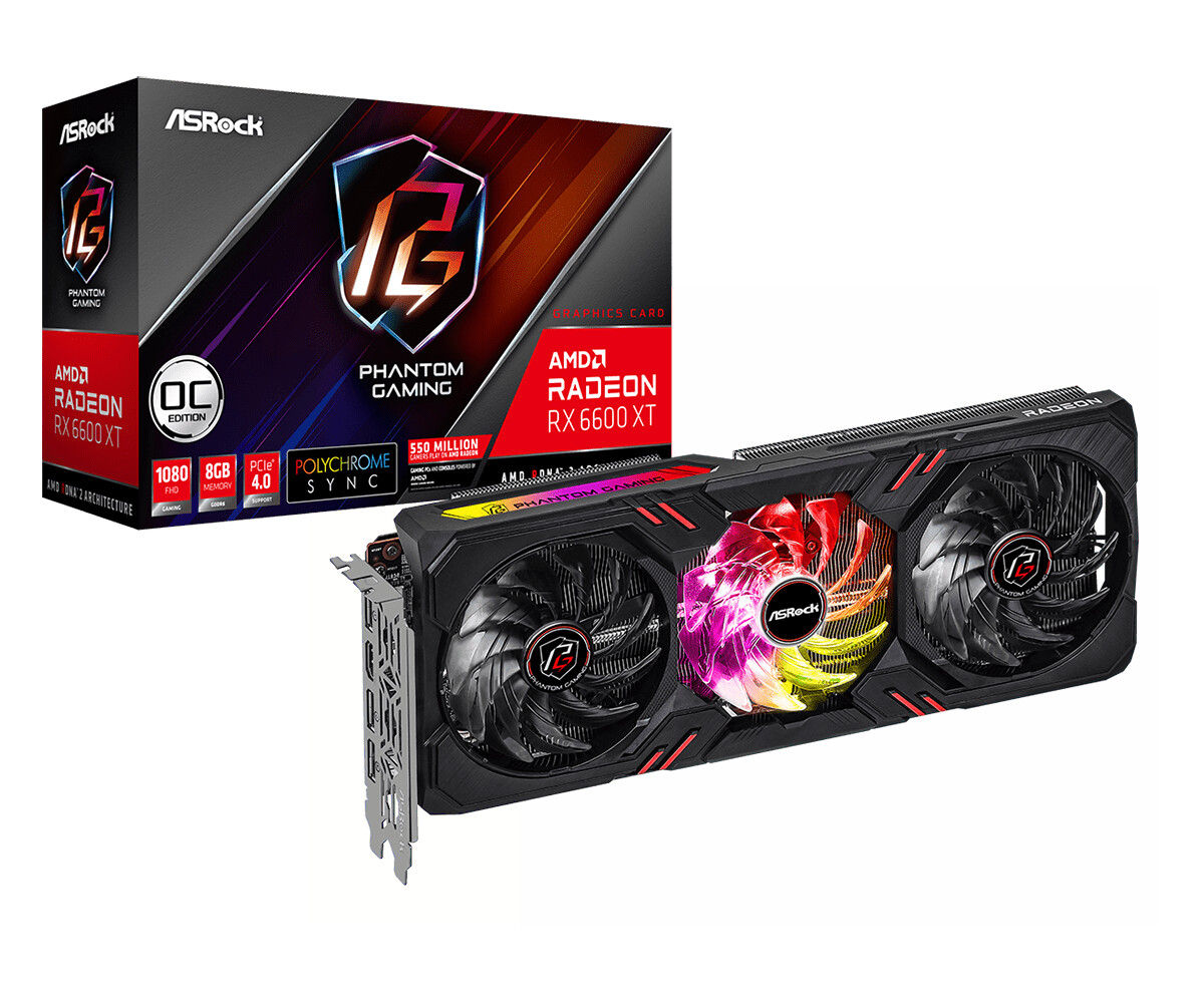
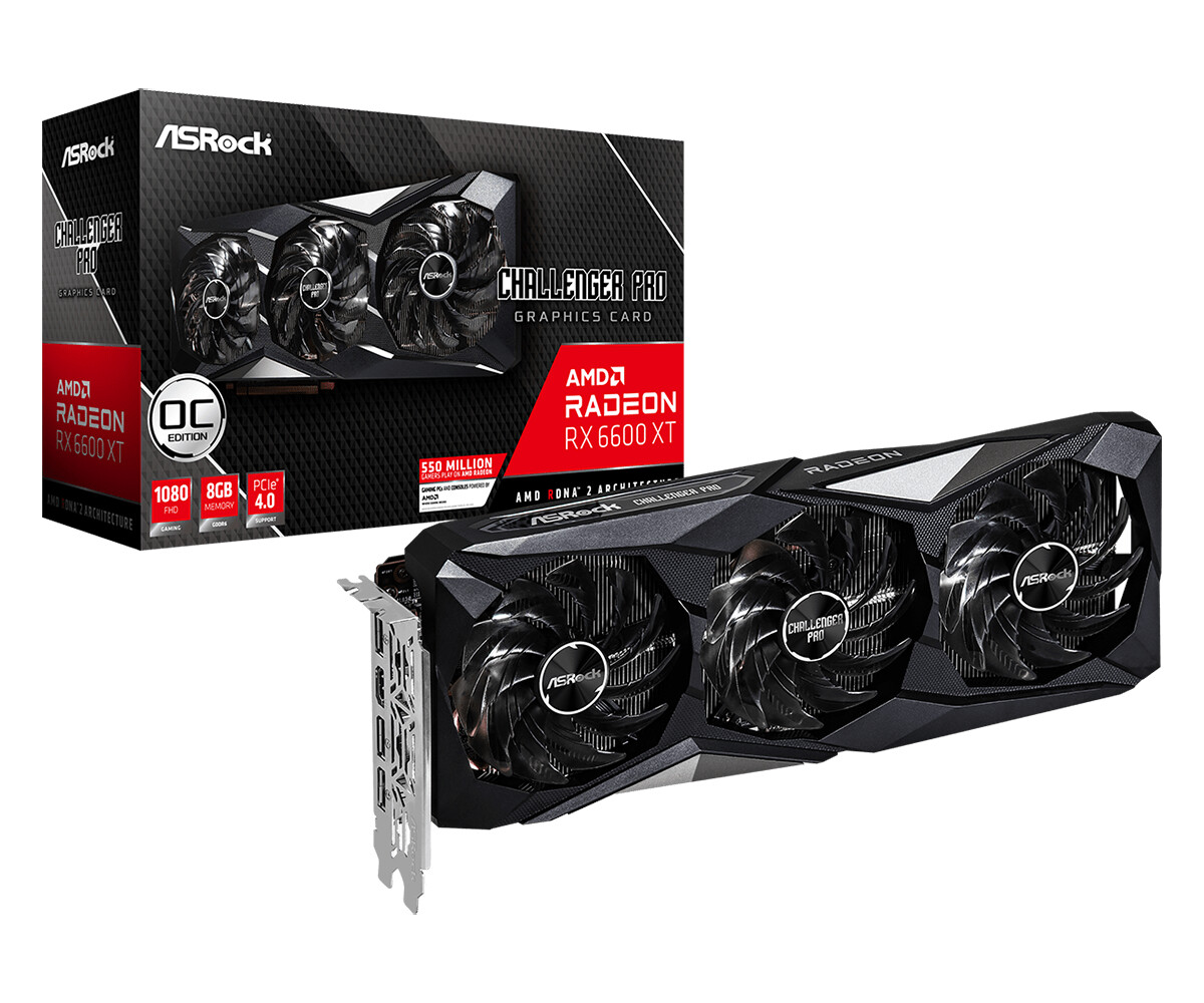
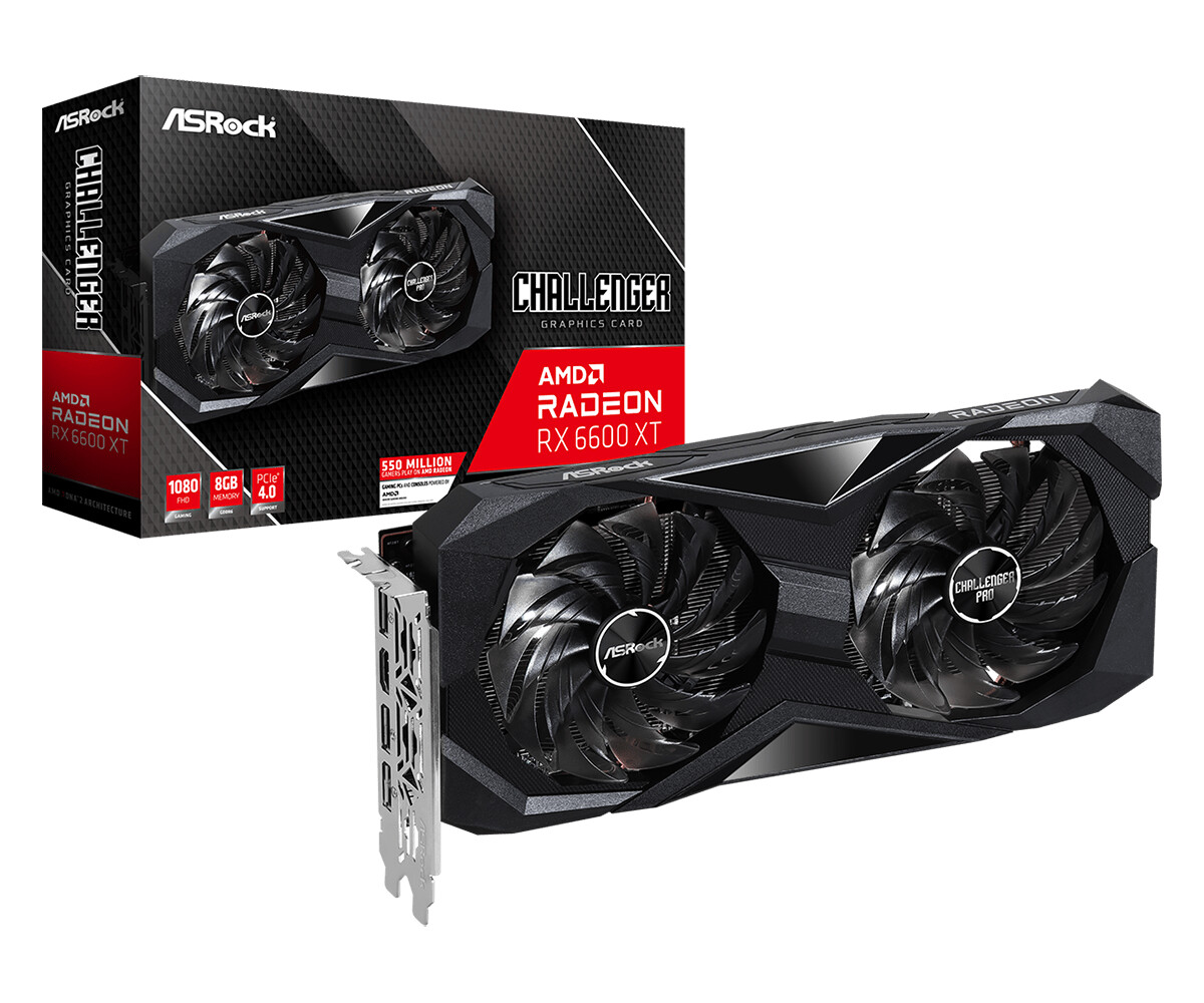
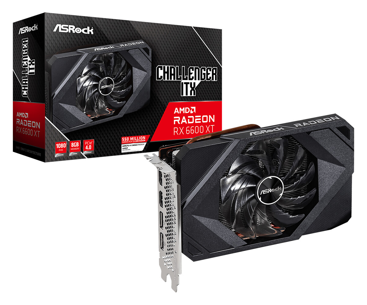
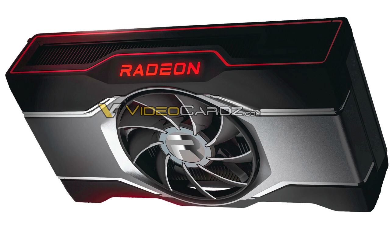
ASRock Announces Radeon RX 6600 Challenger Series Graphics Cards
ASRock, the leading global motherboard, graphics card and mini PC manufacturer, today launched new Challenger series products based on AMD Radeon RX 6600 GPUs. Built on the 7 nm manufacturing process, the new ASRock graphics cards offer support for the DirectX 12 Ultimate API, hardware-accelerated ray tracing, HDMI 2.1, PCI Express 4.0, and the Microsoft Windows 11 operating system. With a wealth of exclusive features, the new graphics cards are designed to provide visually stunning, high-refresh rate 1080p gaming experiences to the midrange market.
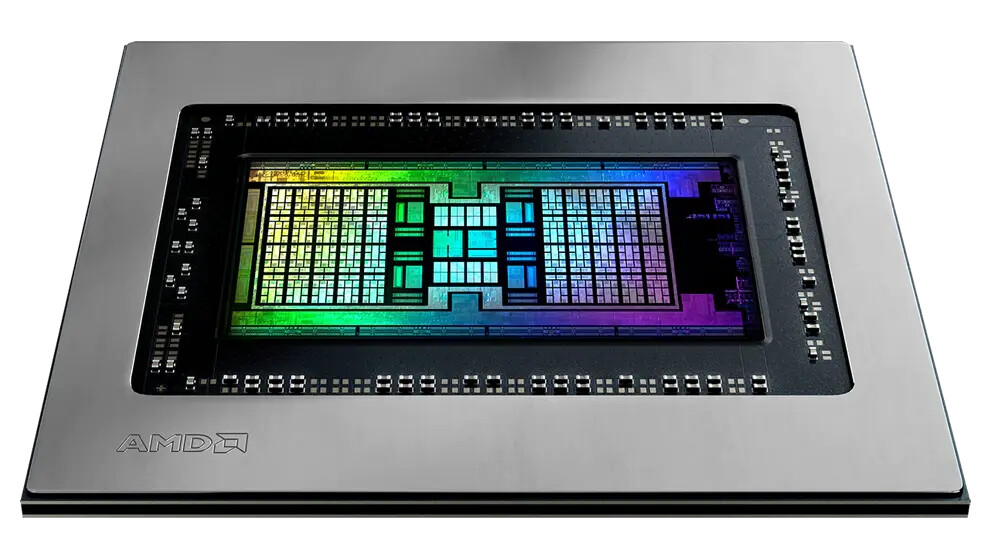
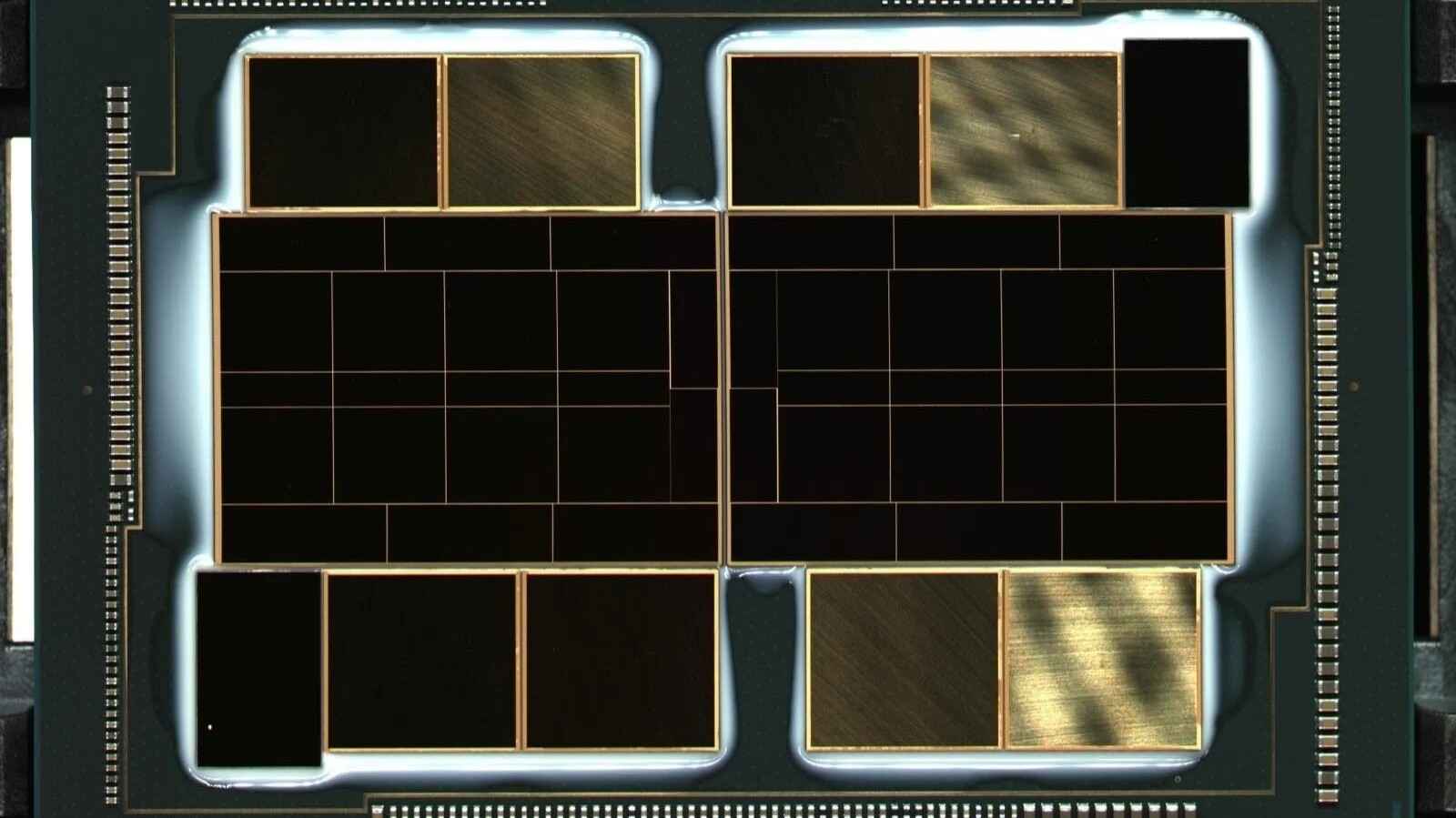
The new graphics cards are built on the breakthrough AMD RDNA 2 gaming architecture, designed to deliver the optimal balance of performance and power efficiency. Offering 32 MB of high-performance AMD Infinity Cache, 8 GB of GDDR6 memory, AMD Smart Access Memory and other advanced features, the new graphics cards are designed to bring next-generation desktop gaming experiences to the midrange market. They also support the AMD FidelityFX Super Resolution open-source spatial upscaling solution, which is designed to increase framerates while delivering high-resolution gaming experiences.

The new graphics cards are built on the breakthrough AMD RDNA 2 gaming architecture, designed to deliver the optimal balance of performance and power efficiency. Offering 32 MB of high-performance AMD Infinity Cache, 8 GB of GDDR6 memory, AMD Smart Access Memory and other advanced features, the new graphics cards are designed to bring next-generation desktop gaming experiences to the midrange market. They also support the AMD FidelityFX Super Resolution open-source spatial upscaling solution, which is designed to increase framerates while delivering high-resolution gaming experiences.