News Posts matching #7 nm

Return to Keyword Browsing

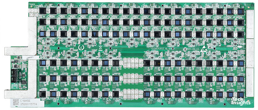
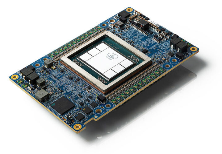
Andes Technology Unveils The AndesCore AX60 Series, An Out-Of-Order Superscalar Multicore RISC-V Processor Family

Today, at Linley Fall Processor Conference 2022, Andes Technology, a leading provider of high efficiency, low power 32/64-bit RISC-V processor cores and founding premier member of RISC-V International, reveals its top-of-the-line AndesCore AX60 series of power and area efficient out-of-order 64-bit processors. The family of processors are intended to run heavy-duty OS and applications with compute intensive requirements such as advanced driver-assistance systems (ADAS), artificial intelligence (AI), augmented/virtual reality (AR/VR), datacenter accelerators, 5G infrastructure, high-speed networking, and enterprise storage.

The first member of the AX60 series, the AX65, supports the latest RISC-V architecture extensions such as the scalar cryptography extension and bit manipulation extension. It is a 4-way superscalar with Out-of-Order (OoO) execution in a 13-stage pipeline. It fetches 4 to 8 instructions per cycle guided by highly accurate TAGE branch predictor with loop prediction to ensure fetch efficiency. It then decodes, renames and dispatches up to 4 instructions into 8 execution units, including 4 integer units, 2 full load/store units, and 2 floating-point units. Besides the load/store units, the AX65's aggressive memory subsystem also includes split 2-level TLBs with multiple concurrent table walkers and up to 64 outstanding load/store instructions.

TSMC Cuts Back CAPEX Budget Despite Record Profits

Another quarter, another record breaking earnings report by TSMC, but it seems like the company has released that things are set to slow down sooner than initially expected and the company is hitting the brakes on some of its expansion projects. The company saw a 79.7 percent increase in profits compared to last year, with a profit of US$8.8 billion and a revenue of somewhere between US$19.9 to US$ 20.7 billion for the third quarter, which is a 47.9 percent bump compared to last year. TSMC's 5 nm nodes were the source for 28 percent of the revenues, followed by 26 percent for 7 nm nodes, 12 percent for 16 nm and 10 percent for 28 nm, with remaining nodes at 40 nm and larger making up for the remainder of the revenue. By platform, smartphone chips made up 41 percent, followed by High Performance Computing at 39 percent, IoT at 10 percent and automotive at five percent.

TSMC said it will cut back its CAPEX budget by around US$4 billion, to US$36 billion, compared to the earlier stated US$40 billion budget the company had set aside for expanding its fabs. Part of the reason for this is that TSMC is already seeing weaker demand for products manufactured using its N7 and N6 nodes, as the N7 node was meant to be a key part of the new fab in Kaohsiung in southern Taiwan. TSMC is expecting to start production on its first N3 node later this quarter and is expecting the capacity to be fully utilised for all of 2023. Supply is said to be exceeding demand, which TSMC said is partially to blame on tooling delivery issues. TSMC is expecting next year's revenue for its N3 node to be higher than its N5 node in 2020, although the revenue is said to be in the single digit percentage range. The N3E node is said to start production sometime in the second half of next year, or about a quarter earlier than expected. The N2 node isn't due to start production until 2025, but TSMC is already having very high customer engagement, so it doesn't look like TSMC is likely to suffer from a lack of business in the foreseeable future, as long as the company keeps delivering new nodes as planned.

US Strengthens China Export Bans, Limiting Access to Manufacturing Technology

The US Department of Commerce is in the process of increasing the stranglehold in tech exports directed to Chinese shores. The move is being made through the delivery of letters to US-based technology companies - namely KLA Corp, Lam Research Corp and Applied Materials Inc. - ordering them to stop the export of machines and equipment that can be used for sub-14 nm manufacturing. The move by the Department of Commerce only has validity for the companies that have been served by such a letter - at least until the Department codifies its newest regulations.

This means that only sellers with approved export licenses can keep doing business with Beijing, thus limiting the US companies China can work with as it aims to achieve at least a degree of self-sufficiency in the latest chipmaking tech. Perhaps the decision has come too late, however, as China's mainstay silicon manufacturing, SMIC, already manufactures chips at the 14 nm process (chips that have been deployed in China's Tinahu Light supercomputer already) and has even showcased manufacturing capability in the 7 nm field. It pays to remember that the US already had applied similar restrictions on equipment experts to China for the better part of two years - which apparently did little to stem China's capability to create increasingly denser semiconductor designs.

BIREN BR100 Detailed: China's AI-HPC Processor Storms into the HPC GPU Big Leagues

If InnoSilicon's Fenghua gaming GPU hit the scene last November seemingly out of nowhere, then another Chinese GPU developer is making waves at HotChips 22, this time in the enterprise space. The BR100 by BIREN is a large AI-HPC GPU-based processor that's China's answer to the Hopper, Ponte Vecchio, and CDNA2, and ensure China's growth as an AI/HPC leader is unaffected in the event of a tech embargo for whatever reason.

The BR100 is an MCM of two planar-silicon dies built on the 7 nm DUV node, with a striking 77 billion transistor-count between them, and 550 W TDP (typical). The chip features 64 GB of on-package HBM2E memory. System bus interfaces include PCI-Express 5.0 x16 with CXL, and eight lanes of a proprietary interconnect called B-Link, which total 2.3 TB/s of bandwidth. The processor supports nearly all popular compute formats except double-precision floating-point, or FP64. Among the supported ones are single-precision or FP32, TF32+, FP16, BF16, INT16, and INT8. BIREN claims up to 256 TFLOP/s FP32, up to 512 TFLOP/s TF32+, up to 1 PFLOP/s BF16, and 2,048 TOPS INT8. This would put it at 2.4 to 2.8 times faster than NVIDIA's "Ampere" A100.

AMD Readies a Handful New Ryzen PRO 5000 Desktop Processor SKUs

AMD is readying a handful new Ryzen PRO 5000 series desktop processor models, according to a leaked Lenovo datasheet for commercial desktops. These Socket AM4 processors are based on either the 7 nm "Renoir" monolithic silicon with "Zen 2" CPU cores; or the "Vermeer" MCM with "Zen 3" cores; all feature 65 W TDP, and the AMD PRO feature-set that rivals Intel vPro, including a framework for remote management, AMD PRO Security, PRO Manageability, and PRO Business (a priority tech-support channel).

Models in the lineup include the Ryzen 3 PRO 4350G, a "Renoir" based APU with a 4-core/8-thread "Zen 2" CPU clocked up to 4.00 GHz, and Radeon Vega 6 integrated graphics. The Ryzen 5 PRO 5645 is based on "Vermeer," and is a 6-core/12-thread "Zen 3" processor with 32 MB of L3 cache, and up to 4.60 GHz clock speeds. The Ryzen 7 PRO 5845 is the 8-core/16-thread model in the lineup, clocked up to 4.60 GHz. Leading the pack is the Ryzen 9 5945, a 12-core/24-thread chip clocked up to 4.70 GHz. From the looks of it, these processors will be exclusively available in the OEM channel, but AMD's OEM-only chips inevitably end up in the retail channel where they're sold loose from trays.

Chinese SMIC Ships 7 nm Chips, Reportedly Copied TSMC's Design

The Chinese technology giant, SMIC, has managed to advance its semiconductor manufacturing technology and shipped the first 7 nm silicon manufactured on China's soil. According to analyst firm TechInsights, who examined the 7 nm Bitcoin mining SoC made for MinerVa firm, there are doubts that SMIC 7 nm process is somewhat similar to TSMC's 7 nm process. Despite having no access to advanced semiconductor manufacturing tools, and US restrictions placed around it, SMIC has managed to produce what resembles an almost perfect 7 nm node. This could lead to a true 7 nm logic and memory bitcells sometimes in the future, as the node advances in SMIC's labs.

Having done an in-depth die analysis, the TechInsights report indicates that TSMC, Intel, and Samsung have a more advanced 7 nm node and are two nodes ahead of the Chinese SMIC. The results are not great regarding the economics and yield of this SMIC 7 nm process. While we have no specific data, the report indicates that the actual working chips made with older DUV tools are not perfect. This is not a problem for the Chinese market as it seeks independence from Western companies and technology. However, introducing a China-made 7 nm chip is more critical as it shows that the country can manufacture advanced nodes with restrictions and sanctions in place. The MinerVa SoC die and the PCB that houses those chips are pictured below.

TSMC Reports Second Quarter EPS of NT$9.14

TSMC (TWSE: 2330, NYSE: TSM) today announced consolidated revenue of NT$534.14 billion, net income of NT$237.03 billion, and diluted earnings per share of NT$9.14 (US$1.55 per ADR unit) for the second quarter ended June 30, 2022. Year-over-year, second quarter revenue increased 43.5% while net income and diluted EPS both increased 76.4%. Compared to first quarter 2022, second quarter results represented an 8.8% increase in revenue and a 16.9% increase in net income. All figures were prepared in accordance with TIFRS on a consolidated basis.

In US dollars, second quarter revenue was $18.16 billion, which increased 36.6% year-over-year and increased 3.4% from the previous quarter. Gross margin for the quarter was 59.1%, operating margin was 49.1%, and net profit margin was 44.4%. In the second quarter, shipments of 5-nanometer accounted for 21% of total wafer revenue; 7- nanometer accounted for 30%. Advanced technologies, defined as 7-nanometer and more advanced technologies, accounted for 51% of total wafer revenue.

Semiconductor Fab Order Cancellations Expected to Result in Reduced Capacity Utilization Rate in 2H22

According to TrendForce investigations, foundries have seen a wave of order cancellations with the first of these revisions originating from large-size Driver IC and TDDI, which rely on mainstream 0.1X μm and 55 nm processes, respectively. Although products such as MCU and PMIC were previously in short supply, foundries' capacity utilization rate remained roughly at full capacity through their adjustment of product mix. However, a recent wave cancellations have emerged for PMIC, CIS, and certain MCU and SoC orders. Although still dominated by consumer applications, foundries are beginning to feel the strain of the copious order cancellations from customers and capacity utilization rate has officially declined.

Looking at trends in 2H22, TrendForce indicates, in addition to no relief from the sustained downgrade of driver IC demand, inventory adjustment has begun for smartphones, PCs, and TV-related peripheral components such as SoCs, CIS, and PMICs, and companies are beginning to curtail their wafer input plans with foundries. This phenomenon of order cancellations is occurring simultaneously in 8-inch and 12-inch fabs at nodes including 0.1X μm, 90/55 nm, and 40/28 nm. Not even the advanced 7/6 nm processes are immune.

Intel 4 Process Node Detailed, Doubling Density with 20% Higher Performance

Intel's semiconductors nodes have been quite controversial with the arrival of the 10 nm design. Years in the making, the node got delayed multiple times, and only recently did the general public get the first 10 nm chips. Today, at IEEE's annual VLSI Symposium, we get more details about Intel's upcoming nodes, called Intel 4. Previously referred to as a 7 nm process, Intel 4 is the company's first node to use EUV lithography accompanied by various technologies. The first thing when a new process node is discussed is density. Compared to Intel 7, Intel 4 will double the transistor count for the same area and enable 20% higher performing transistors.

Looking at individual transistor size, the new Intel 4 node represents a very tiny piece of silicon that is even smaller than its predecessor. With a Fin Pitch of 30 nm, Contact Gate Poly Pitch of 50 nm between gates, and Minimum Metal Pitch (M0) of 50 nm, the Intel 4 transistor is significantly smaller compared to the Intel 7 cell, listed in the table below. For scaling, Intel 4 provides double the number of transistors in the same area compared to Intel 7. However, this reasoning is applied only to logic. For SRAM, the new PDK provides 0.77 area reduction, meaning that the same SoC built on Intel 7 will not be half the size of Intel 4, as SRAM plays a significant role in chip design. The Intel 7 HP library can put 80 million transistors on a square millimeter, while Intel 4 HP is capable of 160 million transistors per square millimeter.

Sapphire Radeon 6700 Graphics Cards Real: No RX, No XT

Sapphire formally launched its Radeon 6700 series graphics card. The AMD Radeon 6700 is an odd-ball SKU that doesn't yet feature in the company's retail product stack, but is yet being released to retail by Sapphire. So far we've not come across any other board partner with this SKU. The 6700 is unique in its branding—there's neither "RX" nor "XT" in the model name, it's called simply the "Radeon 6700."

Carved out from the same 7 nm "Navi 22" silicon as the RX 6700 XT and RX 6750 XT; the 6700 has 36 out of 40 compute units enabled, working out to 2,304 stream processors, and 144 TMUs. The card is endowed with 10 GB of 16 Gbps GDDR6 memory across a 160-bit wide memory interface. Sapphire has two cards in its lineup, one is an unnamed base model that sticks to the "reference" specs, and a factory-overclocked Pulse 6700 card.

Habana Labs Launches Second-generation AI Deep Learning Processors

Today at the Intel Vision conference, Habana Labs, an Intel company, announced its second-generation deep learning processors, the Habana Gaudi 2 Training and Habana Greco Inference processors. The processors are purpose-built for AI deep learning applications, implemented in 7nm technology and build upon Habana's high-efficiency architecture to provide customers with higher-performance model training and inferencing for computer vision and natural language applications in the data center. At Intel Vision, Habana Labs revealed Gaudi2's training throughput performance for the ResNet-50 computer vision model and the BERT natural language processing model delivers twice the training throughput over the Nvidia A100-80GB GPU.

"The launch of Habana's new deep learning processors is a prime example of Intel executing on its AI strategy to give customers a wide array of solution choices - from cloud to edge - addressing the growing number and complex nature of AI workloads. Gaudi2 can help Intel customers train increasingly large and complex deep learning workloads with speed and efficiency, and we're anticipating the inference efficiencies that Greco will bring."—Sandra Rivera, Intel executive vice president and general manager of the Datacenter and AI Group

AMD Announces Ryzen 5000C "Zen 3" Processors for Chromebooks

AMD today announced the Ryzen 5000C line of mobile processors for Chromebooks. This is the company's second generation of Chromebook-specific processors after the Ryzen 3000C series based on the original "Zen" microarchitecture. The 5000C series chips are based on "Zen 3," with CPU core counts of up to 8-core, and hence present a big leap in performance over the 3000C series, along with a complete suite of the latest connectivity, display technology, and security and management features specific to Chrome OS.

The Ryzen 5000C series is based on the 7 nm "Cezanne" monolithic silicon. The chip physically features an 8-core/16-thread CPU based on the "Zen 3" microarchitecture, with 16 MB of shared L3 cache; an iGPU based on the Vega graphics architecture, with 8 compute units (512 stream processors), a dual-channel DDR4 or LPDDR4/x memory interface, and unlike the conventional Ryzen 5000-series mobile processors, these chips come with a special microcode to match the security and management features of Chrome OS. AMD also supplies Chromebook vendors with timely driver updates for the various components on these chips.

PowerColor Radeon RX 6650 XT Hellhound Specs Sheet Hints at Clock Speed Increases Over RX 6600 XT

A leaked specifications sheet of the upcoming PowerColor Radeon RX 6650 XT Hellhound custom-design graphics card, seen by VideoCards, sheds light on AMD's play at carving out the RX 6650 XT. It involves dialing up the engine clocks (GPU clock speed), and memory bandwidth. At this point it is not known if the RX 6650 XT is based on a refined variant of the "Navi 23" silicon, possibly leveraging the TSMC N6 (6 nm) process, or if it's just a case of AMD dialing up clock speeds while pushing up the typical board power, on existing 7 nm (TSMC N7) process.

The RX 6650 XT Hellhound comes with about 4.3% increase in game clocks in its default "OC mode" BIOS, and about 3.7% increase in maximum boost clocks, up from 2593 MHz to 2689 MHz. The "Silent mode" BIOS of the RX 6650 XT Hellhound offers better clock speeds than the "OC mode" BIOS of the RX 6600 XT Hellhound, at 2410 MHz game, 2635 MHz boost, compared to 2382 MHz game, 2593 MHz boost. The other big surprise is memory clocks, with AMD possibly using 17.5 Gbps GDDR6 memory speeds, compared to 16 Gbps on the RX 6600 XT. This results in a 9.4% increase in memory bandwidth. The RX 6600 XT Hellhound uses a single 8-pin PCIe power connector, for an input capacity of 225 W (including the PCIe slot power), which is sufficient for the card's 160 W typical board power. The TBP of the RX 6650 XT Hellhound is not known, but given that its specs sheet still shows single 8-pin, it has to be under 225 W.

"Navi 31" RDNA3 Sees AMD Double Down on Chiplets: As Many as 7

Way back in January 2021, we heard a spectacular rumor about "Navi 31," the next-generation big GPU by AMD, being the company's first logic-MCM GPU (a GPU with more than one logic die). The company has a legacy of MCM GPUs, but those have been a single logic die surrounded by memory stacks. The RDNA3 graphics architecture that the "Navi 31" is based on, sees AMD fragment the logic die into smaller chiplets, with the goal of ensuring that only those specific components that benefit from the TSMC N5 node (6 nm), such as the number crunching machinery, are built on the node, while ancillary components, such as memory controllers, display controllers, or even media accelerators, are confined to chiplets built on an older node, such as the TSMC N6 (6 nm). AMD had taken this approach with its EPYC and Ryzen processors, where the chiplets with the CPU cores got the better node, and the other logic components got an older one.

Greymon55 predicts an interesting division of labor on the "Navi 31" MCM. Apparently, the number-crunching machinery is spread across two GCD (Graphics Complex Dies?). These dies pack the Shader Engines with their RDNA3 compute units (CU), Command Processor, Geometry Processor, Asynchronous Compute Engines (ACEs), Rendering Backends, etc. These are things that can benefit from the advanced 5 nm node, enabling AMD to the CUs at higher engine clocks. There's also sound logic behind building a big GPU with two such GCDs instead of a single large GCD, as smaller GPUs can be made with a single such GCD (exactly why we have two 8-core chiplets making up a 16-core Ryzen processors, and the one of these being used to create 8-core and 6-core SKUs). The smaller GCD would result in better yields per wafer, and minimize the need for separate wafer orders for a larger die (such as in the case of the Navi 21).

AMD EPYC "Genoa" Zen 4 Processor Multi-Chip Module Pictured

Here is the first picture of a next-generation AMD EPYC "Genoa" processor with its integrated heatspreader (IHS) removed. This is also possibly the first picture of a "Zen 4" CPU Complex Die (CCD). The picture reveals as many as twelve CCDs, and a large sIOD silicon. The "Zen 4" CCDs, built on the TSMC N5 (5 nm EUV) process, look visibly similar in size to the "Zen 3" CCDs built on the N7 (7 nm) process, which means the CCD's transistor count could be significantly higher, given the transistor-density gained from the 5 nm node. Besides more number-crunching machinery on the CPU core, we're hearing that AMD will increase cache sizes, particularly the dedicated L2 cache size, which is expected to be 1 MB per core, doubling from the previous generations of the "Zen" microarchitecture.

Each "Zen 4" CCD is reported to be about 8 mm² smaller in die-area than the "Zen 3" CCD, or about 10% smaller. What's interesting, though, is that the sIOD (server I/O die) is smaller in size, too, estimated to measure 397 mm², compared to the 416 mm² of the "Rome" and "Milan" sIOD. This is good reason to believe that AMD has switched over to a newer foundry process, such as the TSMC N7 (7 nm), to build the sIOD. The current-gen sIOD is built on Global Foundries 12LPP (12 nm). Supporting this theory is the fact that the "Genoa" sIOD has a 50% wider memory I/O (12-channel DDR5), 50% more IFOP ports (Infinity Fabric over package) to interconnect with the CCDs, and the mere fact that PCI-Express 5.0 and DDR5 switching fabric and SerDes (serializer/deserializers), may have higher TDP; which together compel AMD to use a smaller node such as 7 nm, for the sIOD. AMD is expected to debut the EPYC "Genoa" enterprise processors in the second half of 2022.

AMD RX 6950 XT, RX 6750 XT, and RX 6650 XT Pictured, Launching on May 10

AMD's Radeon RX product stack refresh for Spring-Summer, is reportedly set to launch on May 10, 2022. Here's the first picture of what a reference-design RX 6950 XT flagship, RX 6750 XT, and the mid-range RX 6650 XT, could look like. These reference board designs are essentially identical to the original RX 6000 made-by-AMD (MBA) reference designs, but ditch the two-tone silver+black color-scheme for an all-black scheme with some diamond-cut edges around the fan vents, and some piano-black accents.

At this point it is not known if this refresh sees the Navi 20-series ASICs optically-shrunk to the TSMC N6 (6 nm) silicon fabrication node, or if it's the existing 7 nm ASICs with their total graphics power (TGP) values dialed up to make room for increased engine clocks, and faster 18 Gbps-rated GDDR6 memory chips. It's interesting to see the RX 6750 XT now come with a triple-fan cooler that resembles the RX 6800 (non-XT) cooler in design, if not color. We're not sure if the RX 6650 XT reference design will ever make it to the real-world, or if it's just a concept, and the SKU is an AIB-exclusive (custom-designs only).

AMD Readies Even More Ryzen 5000 Series Desktop SKUs for April

Earlier this week, we learned about AMD making several additions to its Ryzen 5000 Socket AM4 desktop processor lineup, to better compete against the bulk of the 12th Gen Intel Core "Alder Lake" processors. It turns out that there are three more additions to the lineup that we missed, because they're slated for a slightly later availability from the other chips (later by weeks).

The first of these three is the Ryzen 7 5700 (non-X). This chip is uniquely different from the Ryzen 7 5700X and the Ryzen 7 5600G. It is an 8-core/16-thread processor that's based on the 7 nm "Cezanne" silicon, with its iGPU disabled. This means you still get eight "Zen 3" CPU cores, but no iGPU, just 16 MB of L3 cache, and the PCI-Express interface of the chip is limited Gen 3. The Ryzen 3 5100 is the spiritual successor to the very interesting Ryzen 3 3100. It is a 4-core/8-thread processor based on the same "Cezanne" silicon with "Zen 3" cores, but with only 8 MB of L3 cache, and the iGPU remaining disabled. The third chip on the anvil is the Ryzen 7 4700, an interesting 8-core/16-thread offering based on the older "Renoir" silicon with "Zen 2" CPU cores.

Introducing Intel Agilex M-Series FPGAs

With the exponential growth of data in the world today, coupled with the shift from centralized clusters of compute and data storage to a more distributed architecture that processes data everywhere—in the cloud, at the edge, and at all points in between—Field-Programmable Gate Arrays (FPGAs) are taking on an increasingly important role in modern applications from the data center to the network to the edge. The flexibility, power efficiency, massively parallel architecture, and huge input/output (I/O) bandwidth make FPGAs attractive for accelerating a wide range of tasks from high-performance computing (HPC) to storage and networking. Many of these applications put enormous demands on memory, including capacity, bandwidth, latency and power efficiency.

To handle these high-demand applications, Intel today introduced product details for the Intel Agilex M-Series FPGAs, built on Intel 7 process technology, the industry's highest memory bandwidth FPGAs with in-package HBM DRAM. The Intel Agilex M-Series incorporates several new functional innovations and features that provide the industry with the high-speed networking, computing and memory acceleration required to meet ever-more ambitious performance and capability goals for networks, cloud and embedded edge applications.

Intel "Meteor Lake" and "Arrow Lake" Use GPU Chiplets

Intel's upcoming "Meteor Lake" and "Arrow Lake" client mobile processors introduce an interesting twist to the chiplet concept. Earlier represented in vague-looking IP blocks, new artistic impressions of the chip put out by Intel shed light on a 3-die approach not unlike the Ryzen "Vermeer" MCM that has up to two CPU core dies (CCDs) talking to a cIOD (client IO die), which handles all the SoC connectivity; Intel's design has one major difference, and that's integrated graphics. Apparently, Intel's MCM uses a GPU die sitting next to the CPU core die, and the I/O (SoC) die. Intel likes to call its chiplets "tiles," and so we'll go with that.

The Graphics tile, CPU tile, and the SoC or I/O tile, are built on three different silicon fabrication process nodes based on the degree of need for the newer process node. The nodes used are Intel 4 (optically 7 nm EUV, but with characteristics of a 5 nm-class node); Intel 20A (characteristics of 2 nm), and external TSMC N3 (3 nm) node. At this point we don't know which tile gets what. From the looks of it, the CPU tile has a hybrid CPU core architecture made up of "Redwood Cove" P-cores, and "Crestmont" E-core clusters.

AMD Radeon RX 6x50 XT Series Possibly in June-July, RX 6500 in May

AMD's final refresh of the RDNA2 graphics architecture, the Radeon RX 6x50 series, could debut in June or July 2022, according to Greymon55, a reliable source with GPU leaks. The final refresh of RDNA2 could see AMD use faster 18 Gbps GDDR6 memory across the board, and eke out higher engine clocks on existing silicon IP. At this point it's not known if these new chips will be built on the same 7 nm process, or are an optical shrink to 6 nm (TSMC N6). Such a shrink to a node that offers 18% higher transistor density, would have significant payoffs with clock-speed headroom. AMD's RDNA3-based 5 nm GPUs could debut only toward the end of the year.

In related news, AMD is preparing to launch another entry-level SKU within the RX 6000 series; the Radeon RX 6500 (non-XT). Based on the same 6 nm Navi 24 silicon as the RX 6500 XT, this SKU could have a core-configuration that's in-between the RX 6500 XT and the RX 6400, in featuring 768 stream processors across 12 compute units; and 4 GB of GDDR6 memory, which is similar to the RX 6400, but with higher engine clocks. The RX 6500 is targeting a $150 (MSRP) price-point.

TSMC Sees Record Q4 Profits, Plans to Increase CapEx

TSMC has held its quarterly earnings conference today and it's good news all around, at least if you're TSMC or one of its shareholders, as the company reported record profits of US$6.01 billion for the quarter, or an increase of 16.4 percent compared to the same quarter last year. At the same time, the company announced that it's going to increase its CapEx, by no less than US$40-44 billion this year, which should be compared to the US$30 billion in 2021. The company is expecting to continue to rake in money this quarter, with an expected revenue before expenditures and tax of US$16.6 to US$17.2 billion, compared to US$15.74 billion for this quarter.

Looking at the graphs provided by TSMC which shows where its revenue is coming from, its 7 nm and 5 nm nodes are now accounting for 50 percent of TSMC's revenues. The 5 nm node on its own, almost made as much money as its 16 and 28 nm nodes combined in Q4. We can also see that the 5 nm has gone from eight percent of TSMC's revenues in 2020, to 19 percent this year, with the 7 nm node dropping slightly from 33 percent to 31 percent. 2021 saw a massive 51 percent revenue growth in automotive components for TSMC compared to 2020, yet it only accounted for four percent of TSMC's total revenue for 2021. Smartphones and HPC are jointly holding 81 percent of TSMC's business based on revenue, which isn't likely to change any time soon.

XFX BC-160 Mining Card Based on "Navi 12" Sells in China for $2,000

XFX started selling the AMD BC-160 cryptocurrency mining card based on the AMD "Navi 12" silicon. The card is available on AliExpress for $2,000. The "Navi 12," if you recall, is an MCM mobile GPU that AMD developed exclusively for the 2019 MacBook Pro. It combined an RDNA-based GPU die with up to 16 GB of HBM2 across a 2048-bit wide interface. Built on the 7 nm node, the GPU die of "Navi 12" on the BC-160 is configured with 36 compute units (2,304 stream processors), and 8 GB of HBM2 across the full 2048-bit memory bus.

The card uses a blower-type cooling solution, and is rated with 150 W of typical board power, with a claimed 69.5 Mh/s (ETH). Drivers are provided for Linux, and mining software supported include Team Red Miner and Phoenix Miner. The card features a PCI-Express 4.0 x16 interface, its driver supports systems with up to 12 of these installed. A marketing slide sheds light on the nomenclature AMD is using for its mining cards. The "BC" in BC-160 represents "blockchain compute," the "1" stands for generation, in this case, first generation; and "60" represents hashrate-class with ETH.

AMD Prepares 7nm "Renoir X" Processors Lacking Integrated Graphics, and "Vermeer S"

AMD apparently finds itself with quite a bit of undigested 7 nm "Renoir" silicon, which it plans to repackage as Socket AM4 processors, reports VideoCardz, citing sources on ChipHell forums. The most interesting aspect of this leak is that the silicon variant, codenamed "Renoir X," comes with a disabled iGPU. This is hence a case of AMD harvesting enough "Renoir" dies with faulty iGPU components, to sell them off as desktop processors. It is also learned that these chips don't feature all of the 8 "Zen 2" CPU cores present on the silicon, but rather AMD is looking to carve out entry-level SKUs, such as the Ryzen 3 or Athlon. The company lacks Athlon desktop SKUs based on "Zen 2" or later, although traditionally the company sought to include some basic iGPU solution with its Athlon SKUs.

In related news, the source reports that AMD will refresh its Ryzen desktop processor family with the new "Vermeer S" Ryzen processors. Built on the existing Socket AM4 package, these use AMD's "Zen 3" CCDs that feature 3D Vertical Cache (3DV Cache), much like the recently announced EPYC "Milan X" server processors. AMD claimed that the 3DV Cache technology has a significant performance uplift on performance akin to a generational update. These could be the company's first response to Intel Core "Alder Lake," although since they're based on the older AM4 platform, could only feature DDR4 and PCIe Gen 4. Much like the Ryzen 3000XT series, these appear to be a stopgap product lineup, with AMD targeting late-Q2/early-Q3 for next-generation "Raphael" Socket AM5 processors based on the "Zen 4" architecture, with DDR5 and PCIe Gen 5.

Intel "Meteor Lake" Chips Already Being Built at the Arizona Fab

With its 12th Gen Core "Alder Lake-P" mobile processors still on the horizon, Intel is already building test batches of the 14th Gen "Meteor Lake" mobile processors, at its Fab 42 facility in Chandler, Arizona. "Meteor Lake" is a multi-chip module that leverages Intel's Foveros packaging technology to combine "tiles" (purpose built dies) based on different silicon fabrication processes depending on their function and transistor-density/power requirements. It combines four distinct tiles across a single package—the compute tile, with the CPU cores; the graphics tile with the iGPU: the SoC I/O tile, which handles the processor's platform I/O; and a fourth tile, which is currently unknown. This could be a memory stack with similar functions as the HBM stacks on "Sapphire Rapids," or something entirely different.

The compute tile contains the processor's various CPU core types. The P cores are "Redwood Cove," which are two generations ahead of the current "Golden Cove." If Intel's 12-20% generational IPC uplift cadence holds, we're looking at cores with up to 30% higher IPC than "Golden Cove" (50-60% higher than "Skylake."). "Meteor Lake" also debuts Intel's next-generation E-core, codenamed "Crestmont." The compute tile is rumored to be fabricated on the Intel 4 node (optically a 7 nm-class node, but with characteristics similar to TSMC N5).

AMD Readies MI250X Compute Accelerator with 110 CUs and 128 GB HBM2E

AMD is preparing an update to its compute accelerator lineup with the new MI250X. Based on the CDNA2 architecture, and built on existing 7 nm node, the MI250X will be accompanied by a more affordable variant, the MI250. According to leaks put out by ExecutableFix, the MI250X packs a whopping 110 compute units (7,040 stream processors), running at 1.70 GHz. The package features 128 GB of HBM2E memory, and a package TDP of 500 W. As for speculative performance numbers, it is expected to offer double-precision (FP64) throughput of 47.9 TFLOP/s, ditto full-precision (FP32), and 383 TFLOP/s half-precision (FP16 and BFLOAT16). AMD's MI200 "Aldebaran" family of compute accelerators are expected to square off against Intel's "Ponte Vecchio" Xe-HPC, and NVIDIA Hopper H100 accelerators in 2022.
Return to Keyword Browsing
Jul 10th, 2025 02:29 CDT change timezone

New Forum Posts

Popular Reviews

TPU on YouTube

Controversial News Posts