News Posts matching #HPC

Return to Keyword Browsing

AMD Says Not to Count on Exotic Materials for CPUs in the Next Ten Years, Silicon Is Still Computing's Best Friend

AMD's senior VP of AMD's datacentre group Forrest Norrod, at the Rice Oil and Gas HPC conference, said that while graphene does have incredible promise for the world of computing, it likely will take some ten years before such exotic material are actually taken advantage off. As Norrod puts it, silicon still has a pretty straightforward - if increasingly complex - path down to 3 nanometer densities. And according to him, at the rate manufacturers are being able to scale down their production nodes further, the average time between node transitions stands at some four or five years - which makes the jump to 5 nm and then 3 nm look exactly some 10 years from now, where Norrod expects to go through two additional shrinking nodes for the manufacturing process.

Of course, graphene is being hailed as the next best candidate for taking over silicon's place at the heart of our more complex, high-performance electronics, due, in part, to its high conductivity independent of temperature variation and its incredible switching resistance - it has been found to be able to operate at Terahertz switching speeds. It's a 2D material, which means that implementations of it will have to occur in deposited sheets of graphene across some other material.

Advantech Unveils New Lineup of SQRAM DDR4 32GB Unbuffered Memory for HPC

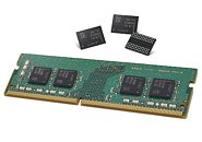
Advantech, a leading global flash storage and memory solutions provider in the embedded market, announces the industry's most comprehensive lineup of 32GB DDR4 unbuffered DIMM memory. Advantech SQRAM offers single 32GB DRAM modules in various DIMM types including SODIMM, UDIMM, ECC DIMM, and extremely robust Rugged DIMM with guaranteed wide temperature operation for high performance computing in applications such as networking and military.

As the global IoT market gradually embraces big data and edge computing, demand for high data and performance processing is increasing. SQRAM 32 GB unbuffered DIMM memory uses Samsung's 16 Gb 2666 MT/s IC chips for high reliability requirements in mission critical applications. SQRAM 32 GB wide temperature operation (-40~85 °C) Rugged DIMM offers extreme vibration resistance, plus ECC checking to ensure data accuracy.

Stuttgart-based HLRS to Build a Supercomputer with 10,000 64-core Zen 2 Processors

Höchstleistungsrechenzentrum (HLRS, or High-Performance Computing Center), based in Stuttgart Germany, is building a new cluster supercomputer powered by 10,000 AMD Zen 2 "Rome" 64-core processors, making up 640,000 cores. Called "Hawk," the supercomputer will be HLRS' flagship product, and will open its doors to business in 2019. The slide-deck for Hawk makes a fascinating disclosure about the processors it's based on.

Apparently, each of the 64-core "Rome" EPYC processors has a guaranteed clock-speed of 2.35 GHz. This would mean at maximum load (with all cores loaded 100%), the processor can manage to run at 2.35 GHz. This is important, because the supercomputer's advertised throughput is calculated on this basis, and clients draw up SLAs on throughput. The advertised peak throughput for the whole system is 24.06 petaFLOP/s, although the company is yet to put out nominal/guaranteed performance numbers (which it will only after first-hand testing). The system features 665 TB of RAM, and 26,000 TB of storage.

Intel Puts Out Additional "Cascade Lake" Performance Numbers

Intel late last week put out additional real-world HPC and AI compute performance numbers of its upcoming "Cascade Lake" 2x 48-core (96 cores in total) machine, compared to AMD's EPYC 7601 2x 32-core (64 cores in total) machine. You'll recall that on November 5th, the company put out Linpack, System Triad, and Deep Learning Inference numbers, which are all synthetic benchmarks. In a new set of slides, the company revealed a few real-world HPC/AI application performance numbers, including MIMD Lattice Computation (MILC), Weather Research and Forecasting (WRF), OpenFOAM, NAMD scalable molecular dynamics, and YaSK.

The Intel 96-core setup with 12-channel memory interface belts out up to 1.5X performance in MILC, up to 1.6X in WRF and OpenFOAM, up to 2.1X in NAMD, and up to 3.1X in YASK, compared to an AMD EPYC 7601 2P machine. The company also put out system configuration and disclaimer slides with the usual forward-looking CYA. "Cascake Lake" will be Intel's main competitor to AMD's EPYC "Rome" 64-core 4P-capable processor that comes out by the end of 2018. Intel's product is a multi-chip module of two 24~28 core dies, with a 2x 6-channel DDR4 memory interface.

AMD and Xilinx Announce a New World Record for AI Inference

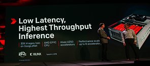
At today's Xilinx Developer Forum in San Jose, Calif., our CEO, Victor Peng was joined by the AMD CTO Mark Papermaster for a Guinness. But not the kind that comes in a pint - the kind that comes in a record book. The companies revealed the AMD and Xilinx have been jointly working to connect AMD EPYC CPUs and the new Xilinx Alveo line of acceleration cards for high-performance, real-time AI inference processing. To back it up, they revealed a world-record 30,000 images per-second inference throughput!

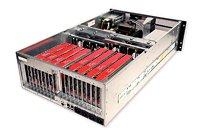
The impressive system, which will be featured in the Alveo ecosystem zone at XDF today, leverages two AMD EPYC 7551 server CPUs with its industry-leading PCIe connectivity, along with eight of the freshly-announced Xilinx Alveo U250 acceleration cards. The inference performance is powered by Xilinx ML Suite, which allows developers to optimize and deploy accelerated inference and supports numerous machine learning frameworks such as TensorFlow. The benchmark was performed on GoogLeNet, a widely used convolutional neural network.

AMD Radeon Vega 12 and Vega 20 Listed in Ashes Of The Singularity Database

Back at Computex, AMD showed a demo of their Vega 20 graphics processor, which is produced using a refined 7 nanometer process. We also reported that the chip has a twice-as-wide memory interface, effectively doubling memory bandwidth, and alsomaximum memory capacity. The smaller process promises improvements to power efficiency, which could let AMD run the chip at higher frequencies for more performance compared to the 14 nanometer process of existing Vega.

As indicated by AMD during Computex, the 7 nanometer Vega is a product targeted at High Performance Compute (HPC) applications, with no plans to release it for gaming. As they clarified later, the promise of "7 nanometer for gamers" is for Navi, which follows the Vega architecture. It's even more surprising to see AOTS results for a non-gaming card - my guess is that someone was curious how well it would do in gaming.

Samsung Miniaturizes the Z-SSD to the M.2 Form-factor

Samsung unveiled an M.2 variant of its flagship high-performance Z-SSD. Targeted at workstations, HPCs, and AI servers, the Z-SSD lineup is built around Samsung's proprietary Z-NAND flash memory, that offer "up to 10 times" higher cell read performance than conventional 3D V-NAND (found on drives such as the 960 Pro). This performance is then traded off for the lowest possible latencies and response-times, which can help certain AI applications. The Z-SSD M.2 is built in the M.2-22110 (110 mm-long) form-factor, and features PCI-Express gen 3.0 x4 interface, and takes advantage of the NVMe protocol.

The drive appears to feature an 8-channel controller that's similar to the one that drives the company's PM983 SSD, and not quite the 16-channel controller found on the larger AIC variant of this drive. Available in capacities of 240 GB and 480 GB, the drive offers sequential transfer rates of up to 3200 MB/s reads, with up to 2800 MB/s writes; with an endurance of 30 DWPD. Like its larger siblings, the Z-SSD M.2 comes with a bank of capacitors to offer power-loss protection. The company didn't reveal availability or pricing information.

Italian Multinational Gas, Oil Company Fires Off HPC4 Supercomputer

Eni has launched its new HPC4 supercomputer, at its Green Data Center in Ferrera Erbognone, 60 km away from Milan. HPC4 quadruples the Company's computing power and makes it the world's most powerful industrial system. HPC4 has a peak performance of 18.6 Petaflops which, combined with the supercomputing system already in operation (HPC3), increases Eni's computational peak capacity to 22.4 Petaflops.

According to the latest official Top 500 supercomputers list published last November (the next list is due to be published in June 2018), Eni's HPC4 is the only non-governmental and non-institutional system ranking among the top ten most powerful systems in the world. Eni's Green Data Center has been designed as a single IT Infrastructure to host all of HPC's architecture and all the other Business applications.

Samsung Now Mass Producing Industry's First 2nd-Generation 10nm Class DRAM

Samsung Electronics Co., Ltd., the world leader in advanced memory technology, announced today that it has begun mass producing the industry's first 2nd-generation of 10-nanometer class (1y-nm), 8-gigabit (Gb) DDR4 DRAM. For use in a wide range of next-generation computing systems, the new 8 Gb DDR4 features the highest performance and energy efficiency for an 8 Gb DRAM chip, as well as the smallest dimensions.

"By developing innovative technologies in DRAM circuit design and process, we have broken through what has been a major barrier for DRAM scalability," said Gyoyoung Jin, president of Memory Business at Samsung Electronics. "Through a rapid ramp-up of the 2nd-generation 10 nm-class DRAM, we will expand our overall 10 nm-class DRAM production more aggressively, in order to accommodate strong market demand and continue to strengthen our business competitiveness."

PCI SIG Releases PCI-Express Gen 4.0 Specifications

The Peripheral Component Interconnect (PCI) special interest group (SIG) published the first official specification (version 1.0) of PCI-Express gen 4.0 bus. The specification's previous draft 0.9 was under technical review by members of the SIG. The new generation PCIe comes with double the bandwidth of PCI-Express gen 3.0, reduced latency, lane margining, and I/O virtualization capabilities. With the specification published, one can expect end-user products implementing it. PCI SIG has now turned its attention to the even newer PCI-Express gen 5.0 specification, which will be close to ready by mid-2019.

PCI-Express gen 4.0 comes with 16 GT/s bandwidth per-lane, per-direction, which is double that of gen 3.0. An M.2 NVMe drive implementing it, for example, will have 64 Gbps of interface bandwidth at its disposal. The SIG has also been steered toward lowering the latencies of the interconnect as HPC hardware designers are turning toward alternatives such as NVLink and InfinityFabric, not primarily for the bandwidth, but the lower latency. Lane margining is a new feature that allows hardware to maintain a uniform physical layer signal clarity across multiple PCIe devices connected to a common root complex. This is particularly important when you have multiple pieces of mission-critical hardware (such as RAID HBAs or HPC accelerators), and require uniform performance across them. The new specification also adds new I/O virtualization features that should prove useful in HPC and cloud computing.

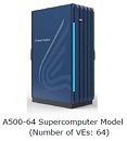
NEC Launches Their SX-Aurora TSUBASA Vector Engine

NEC Corporation (TSE: 6701) today announced the launch of a new high-end HPC product line, the SX-Aurora TSUBASA. This new platform drastically increases processing performance and scalability on real world applications, aiming for the traditional application areas, such as science and engineering, but also targeting the new fields of Machine Learning, Artificial Intelligence and Big Data analytics. With this new technology, NEC opens supercomputing to a wide range of new markets, in addition to the traditional HPC arena.

Utilizing cutting-edge chip integration technology, the new product features a complete multi-core vector processor in the form of a card-type Vector Engine (VE), which is developed based on NEC's high-density interface technology and efficient cooling technology. Kimihiko Fukuda, Executive Vice President, NEC Corporation, said, "The new product addresses the needs of scalar computational capability while still providing the efficiency of a vector architecture. This is accomplished through a tightly integrated complete vector system in the form of a Vector Engine Card."
Samsung Increases Production of 8 GB HBM2 Memory

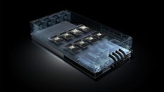
Samsung Electronics Co., Ltd., the world leader in advanced memory technology, today announced that it is increasing the production volume of its 8-gigabyte (GB) High Bandwidth Memory-2 (HBM2) to meet growing market needs across a wide range of applications including artificial intelligence, HPC (high-performance computing), advanced graphics, network systems and enterprise servers.

"By increasing production of the industry's only 8GB HBM2 solution now available, we are aiming to ensure that global IT system manufacturers have sufficient supply for timely development of new and upgraded systems," said Jaesoo Han, executive vice president, Memory Sales & Marketing team at Samsung Electronics. "We will continue to deliver more advanced HBM2 line-ups, while closely cooperating with our global IT customers."

GIGABYTE Releases First Wave Of Products Based On Skylake Purley Architecture

GIGABYTE today announced its latest generation of servers based on Intel's Skylake Purley architecture. This new generation brings a wealth of new options in scalability - across compute, network and storage - to deliver solutions for any application, from the enterprise to the data center to HPC. (Jump ahead to system introductions).

This server series adopts Intel's new product family - officially named the 'Intel Xeon Scalable family' and utilizes its ability to meet the increasingly diverse requirements of the industry, from entry-level HPC to large scale clusters.. The major development in this platform is around the improved features and functionality at both the host and fabric levels. These enable performance improvements - both natively on chip and for future extensibility through compute, network and storage peripherals. In practical terms, these new CPUs will offer up to 28 cores, and 48 PCIe lanes per socket.

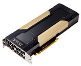
NVIDIA Announces the Tesla V100 PCI-Express HPC Accelerator

NVIDIA formally announced the PCI-Express add-on card version of its flagship Tesla V100 HPC accelerator, based on its next-generation "Volta" GPU architecture. Based on the advanced 12 nm "GV100" silicon, the GPU is a multi-chip module with a silicon substrate and four HBM2 memory stacks. It features a total of 5,120 CUDA cores, 640 Tensor cores (specialized CUDA cores which accelerate neural-net building), GPU clock speeds of around 1370 MHz, and a 4096-bit wide HBM2 memory interface, with 900 GB/s memory bandwidth. The 815 mm² GPU has a gargantuan transistor-count of 21 billion. NVIDIA is taking institutional orders for the V100 PCIe, and the card will be available a little later this year. HPE will develop three HPC rigs with the cards pre-installed.

Could This be the NVIDIA TITAN Volta?

NVIDIA, which unveiled its faster "Volta" GPU architecture at its 2017 Graphics Technology Conference (GTC), beginning with the HPC product Tesla V100, is closer to launching the consumer graphics variant, the TITAN Volta. A curious-looking graphics card image with "TITAN" markings surfaced on Reddit. One could discount the pic for being that of a well-made cooler mod, until you take a peak at the PCB. It appears to lack SLI fingers where you'd expect them to be, and instead has NVLink fingers in positions found on the PCIe add-in card variant of the Tesla P100 HPC accelerator.

You might think "alright, it's not a fancy TITAN X Pascal cooler mod, but it could be a P100 with a cooler mod," until you notice the power connectors - it has two power inputs on top of the card (where they're typically found on NVIDIA's consumer graphics cards), and not the rear portion of the card (where the P100 has it, and where they're typically found on Tesla and Quadro series products). Whoever pulled this off has done an excellent job either way - of scoring a potential TITAN Volta sample, or modding whatever card to look very plausible of being a TITAN Volta.

NVIDIA's Volta Reportedly Poised for Anticipated, Early Q3 2017 Launch

According to a report from Chinese website MyDrivers, NVIDIA is looking to spruce things up on its line-up with a much earlier than expected Q3 Volta Launch. Remember that Volta was expected, according to NVIDIA's own road-maps, to launch around early 2018. The report indicates that NVIDIA's Volta products - apparently to be marketed as the GeForce 20-series - will see an early launch due to market demands, and NVIDIA's intention to further increase pricing of its products through a new-generation launch.

These stand, for now, as only rumors (and not the first time they've surfaced at that), but paint a pretty interesting picture, nonetheless. Like Intel with its Coffee Lake series, pushing a product launch to earlier than expected has consequences: production, logistics, infrastructure, product roadmaps, and stock of existing previous-generation products must all be taken into account. And with NVIDIA just recently having introduced its performance-champions GTX 1080 Ti and Titan Xp graphics cards, all of this seems a trigger pull too early - especially when taking into account the competition landscape in high-performance graphics, which is akin to a single green-colored banner poised atop the Himalayas. And NVIDIA must not forget the fact that AMD could be pulling a black swan off its engineering department with Vega, like it did with its Ryzen series of CPUs.

NVIDIA, Microsoft Launch Industry-Standard Hyperscale GPU Accelerator

NVIDIA with Microsoft today unveiled blueprints for a new hyperscale GPU accelerator to drive AI cloud computing. Providing hyperscale data centers with a fast, flexible path for AI, the new HGX-1 hyperscale GPU accelerator is an open-source design released in conjunction with Microsoft's Project Olympus.

HGX-1 does for cloud-based AI workloads what ATX -- Advanced Technology eXtended -- did for PC motherboards when it was introduced more than two decades ago. It establishes an industry standard that can be rapidly and efficiently embraced to help meet surging market demand. The new architecture is designed to meet the exploding demand for AI computing in the cloud -- in fields such as autonomous driving, personalized healthcare, superhuman voice recognition, data and video analytics, and molecular simulations.

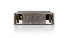
NVIDIA Announces DGX SaturnV: The World's Most Efficient Supercomputer

This week NVIDIA announced their latest innovation to the HPC landscape, the DGX SaturnV. Destined for the likes of universities and companies with a need for deep learning capabilities, the DGX SaturnV sets a new benchmark for energy efficiency in High Performance Computing. While not managing the title of the fastest supercomputer this year, the SaturnV takes a respectable placing of 28th in the top 500 list, while promising much lower running costs for performance on tap.

Capable of delivering 9.46 GFLOPS of computational speed per Watt of energy consumed, it bests last years best effort of 6.67 GFLOPS/W by 42%. The SaturnV is comprised of 125 DGX-1 deep learning systems, and each DGX-1 contains no less than eight Tesla P100 cards. Where a single GTX1080 can churn out 138 GFLOPS of FP16 calculations, a single Telsa P100 can deliver a massive 21.2 TFLOPS. The singular DGX-1 units are already in the field, including being used by NVIDIA themselves.

NVIDIA Tesla P100 Available on Google Cloud Platform

NVIDIA announced that its flagship GPGPU accelerator, the Tesla P100, will be available through Google Cloud Platform. The company's Tesla K80 accelerator will also be offered. The Google Cloud Platform allows customers to perform specific computing tasks at an infinitesimally lower cost than having to rent hardware in-situ or having to buy it; by offloading your computing tasks to offsite data-centers. IT professionals can build and deploy servers, HPC farms, or even supercomputers, of all shapes and sizes within hours of placing an order online with Google.

The Tesla P100 is a GPGPU with the most powerful GPU in existence - the NVIDIA GP100 "Pascal," featuring 3,584 CUDA cores, up to 16 GB of HBM2 memory, and NVLink high-bandwidth interconnect support. The other high-end GPU accelerators on offer by Google are the Tesla K80, based on a pair of GK210 "Kepler" GPUs, and the AMD FirePro S9300 X2, based on a pair of "Fiji" GPUs.

AMD Radeon Technology Will Be Available on Google Cloud Platform in 2017

At SC16, AMD announced that Radeon GPU technology will be available to Google Cloud Platform users worldwide. Starting in 2017, Google will use AMD's fastest available single-precision dual GPU compute accelerators, Radeon-based AMD FirePro S9300 x2 Server GPUs, to help accelerate Google Compute Engine and Google Cloud Machine Learning services. AMD FirePro S9300 x2 GPUs can handle highly parallel calculations, including complex medical and financial simulations, seismic and subsurface exploration, machine learning, video rendering and transcoding, and scientific analysis. Google Cloud Platform will make the AMD GPU resources available for all their users around the world.

"Graphics processors represent the best combination of performance and programmability for existing and emerging big data applications," said Raja Koduri, senior vice president and chief architect, Radeon Technologies Group, AMD. "The adoption of AMD GPU technology in Google Cloud Platform is a validation of the progress AMD has made in GPU hardware and our Radeon Open Compute Platform, which is the only fully open source hyperscale GPU compute platform in the world today. We expect that our momentum in GPU computing will continue to accelerate with future hardware and software releases and advances in the ecosystem of middleware and libraries."

TYAN Displays HPC Platforms for Enterprises and Data Centers

TYAN, an industry-leading server platform design manufacturer and subsidiary of MiTAC Computing Technology Corporation, is showcasing a wide range of HPC server platforms optimized for enterprise, storage and data center applications at SC16 this week in Salt Lake City's Salt Palace Convention Center.

TYAN's comprehensive HPC platforms span a wide range of hardware specifications. The Intel Xeon E7-based, 4U quad-socket FT76-B7922 offers a memory capacity of 6TB and supports up to 4x Intel Xeon Phi coprocessors for the most demanding HPC users; the Intel Xeon E5-based, 4U dual-socket FT77C-B7079 supports up to 8x Intel Xeon Phi coprocessors for highly parallelized application deployment, the 2U dual-socket TA80-B7071 supports up to 4x Intel Xeon Phi coprocessors for large-scale production deployment in various high performance computing segments; and the 1U dual-socket GA80-B7081 supports up to 3x Intel Xeon Phi coprocessors for ISVs, universities, and small businesses looking for parallelized application development or proof of concept solution deployment.

AMD Announces ROCm Initiative - High-Performance Computing & Open-Standards

AMD on Monday announced their ROCm initiative. Introduced by AMD's Gregory Stoner, Senior Director for the Radeon Open Compute Initiative, ROCm stands for Radeon Open Compute platforM. This open-standard, high-performance, Hyper Scale computing platform stands on the shoulders of AMD's technological expertise and accomplishments, with cards like the Radeon R9 Nano achieving as much as 46 GFLOPS of peak single-precision performance per Watt.

The natural evolution of AMD's Boltzmann Initiative, ROCm grants developers and coders a platform which allows the leveraging of AMD's GPU solutions through a variety of popular programming languages, such as OpenCL, CUDA, ISO C++ and Python. AMD knows that the hardware is but a single piece in an ecosystem, and that having it without any supporting software is a recipe for failure. As such, AMD's ROCm stands as AMD's push towards HPC by leveraging both its hardware, as well as the support for open-standards and the conversion of otherwise proprietary code.

NVIDIA Launches Maxed-out GP102 Based Quadro P6000

Late last week, NVIDIA announced the TITAN X Pascal, its fastest consumer graphics offering targeted at gamers and PC enthusiasts. The reign of TITAN X Pascal being the fastest single-GPU graphics card could be short-lived, as NVIDIA announced a Quadro product based on the same "GP102" silicon, which maxes out its on-die resources. The new Quadro P6000, announced at SIGGRAPH alongside the GP104-based Quadro P5000, features all 3,840 CUDA cores physically present on the chip.

Besides 3,840 CUDA cores, the P6000 features a maximum FP32 (single-precision floating point) performance of up to 12 TFLOP/s. The card also features 24 GB of GDDR5X memory, across the chip's 384-bit wide memory interface. The Quadro P5000, on the other hand, features 2,560 CUDA cores, up to 8.9 TFLOP/s FP32 performance, and 16 GB of GDDR5X memory across a 256-bit wide memory interface. It's interesting to note that neither cards feature full FP64 (double-precision) machinery, and that is cleverly relegated to NVIDIA's HPC product line, the Tesla P-series.

NVIDIA Accelerates Volta to May 2017?

Following the surprise TITAN X Pascal launch slated for 2nd August, it looks like NVIDIA product development cycle is running on steroids, with reports emerging of the company accelerating its next-generation "Volta" architecture debut to May 2017, along the sidelines of next year's GTC. The architecture was originally scheduled to make its debut in 2018.

Much like "Pascal," the "Volta" architecture could first debut with HPC products, before moving on to the consumer graphics segment. NVIDIA could also retain the 16 nm FinFET+ process at TSMC for Volta. Stacked on-package memory such as HBM2 could be more readily available by 2017, and could hit sizable volumes towards the end of the year, making it ripe for implementation in high-volume consumer products.

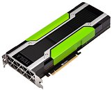
NVIDIA Announces a PCI-Express Variant of its Tesla P100 HPC Accelerator

NVIDIA announced a PCI-Express add-on card variant of its Tesla P100 HPC accelerator, at the 2016 International Supercomputing Conference, held in Frankfurt, Germany. The card is about 30 cm long, 2-slot thick, and of standard height, and is designed for PCIe multi-slot servers. The company had introduced the Tesla P100 earlier this year in April, with a dense mezzanine form-factor variant for servers with NVLink.

The PCIe variant of the P100 offers slightly lower performance than the NVLink variant, because of lower clock speeds, although the core-configuration of the GP100 silicon remains unchanged. It offers FP64 (double-precision floating-point) performance of 4.70 TFLOP/s, FP32 (single-precision) performance of 9.30 TFLOP/s, and FP16 performance of 18.7 TFLOP/s, compared to the NVLink variant's 5.3 TFLOP/s, 10.6 TFLOP/s, and 21 TFLOP/s, respectively. The card comes in two sub-variants based on memory, there's a 16 GB variant with 720 GB/s memory bandwidth and 4 MB L3 cache, and a 12 GB variant with 548 GB/s and 3 MB L3 cache. Both sub-variants feature 3,584 CUDA cores based on the "Pascal" architecture, and core clock speed of 1300 MHz.
Return to Keyword Browsing
Jul 6th, 2025 17:32 CDT change timezone

New Forum Posts

Popular Reviews

TPU on YouTube

Controversial News Posts