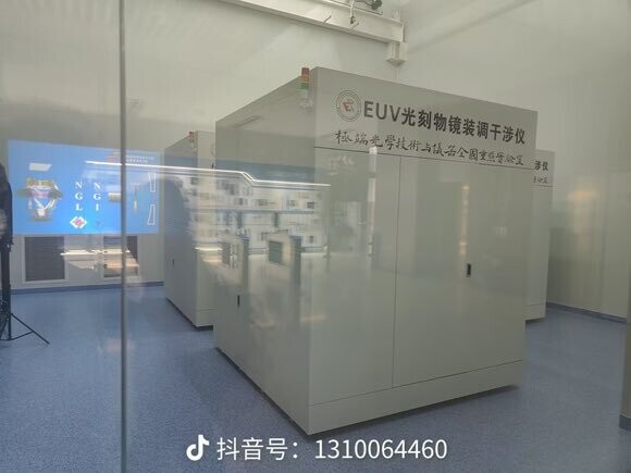
Chinese SiCarrier Shows a Complete Silicon Manufacturing Flow: Deposition, Etching, Metrology, Inspection, and Electrical Testing
SiCarrier, a Huawei-backed Chinese semiconductor tool manufacturer, has launched a comprehensive suite of semiconductor manufacturing tools at this year's Semicon China. These tools are strategically essential to China's semiconductor self-sufficiency and a major step towards competitive nodes from the mainland. The new lineup spans multiple categories: optical inspection, deposition, etch, metrology, and electrical performance testing. Until now, Chinese chipmakers often depended on older-generation foreign equipment, but SiCarrier's new lineup promises domestic alternatives tailored to modern manufacturing processes. The tools address every stage of semiconductor fabrication, from inspecting microscopic defects to etching intricate circuits.
For quality control, SiCarrier's Color Mountain series functions like a high-powered microscope, using intense lighting and advanced imaging algorithms to examine both sides of silicon wafers for flaws as small as dust particles. Complementing this, the Sky Mountain series ensures the perfect alignment of circuit layers, which need perfect stacking, using diffraction-based measurements (analyzing light patterns) and direct image comparisons. The New Mountain suite combines specialized tools to analyze materials at the atomic level. One standout is the atomic force microscope (AFM), which maps surface topography with a nanoscale "finger," while X-ray techniques (XPS, XRD, XRF) act like forensic tools, revealing the chemical composition, crystal structure, and elemental makeup.


For quality control, SiCarrier's Color Mountain series functions like a high-powered microscope, using intense lighting and advanced imaging algorithms to examine both sides of silicon wafers for flaws as small as dust particles. Complementing this, the Sky Mountain series ensures the perfect alignment of circuit layers, which need perfect stacking, using diffraction-based measurements (analyzing light patterns) and direct image comparisons. The New Mountain suite combines specialized tools to analyze materials at the atomic level. One standout is the atomic force microscope (AFM), which maps surface topography with a nanoscale "finger," while X-ray techniques (XPS, XRD, XRF) act like forensic tools, revealing the chemical composition, crystal structure, and elemental makeup.