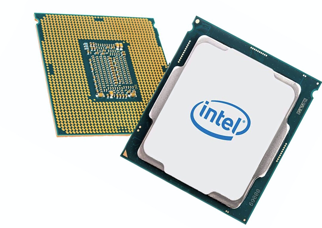
Intel Core i5-10400 Tested, Significant Multi-Threaded Performance Gain Over i5-9400
Intel's upcoming Core i5-10400 processor, priced at USD $184, with an iGPU-devoid i5-10400F variant priced at $157, could be a serious mid-range price-performance package, building on the popularity of its predecessors, the i5-9400F and the i5-8400. The new chip is 6-core/12-thread, with 12 MB of shared L3 cache, or a similar die configuration to the 8th generation Core i7 series. The chip has the same 2.90 GHz nominal clock as the i5-9400, but increases the max Turbo Boost frequency by 200 MHz to 4.30 GHz.
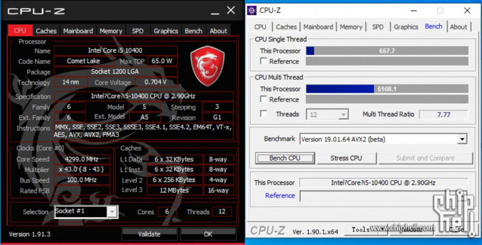
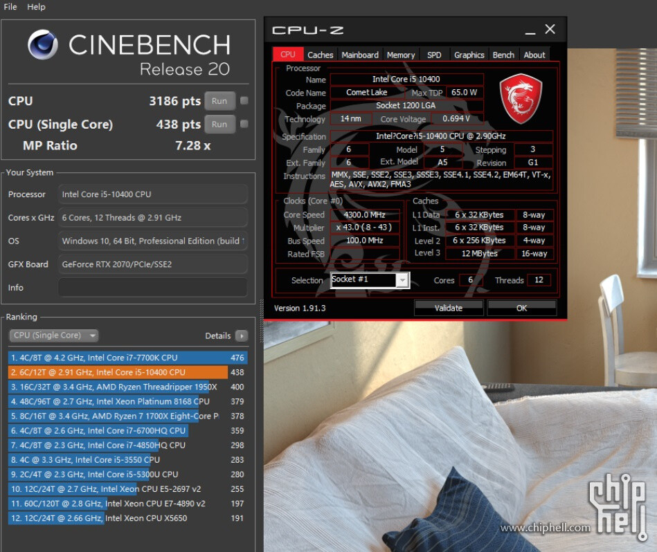
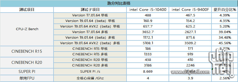
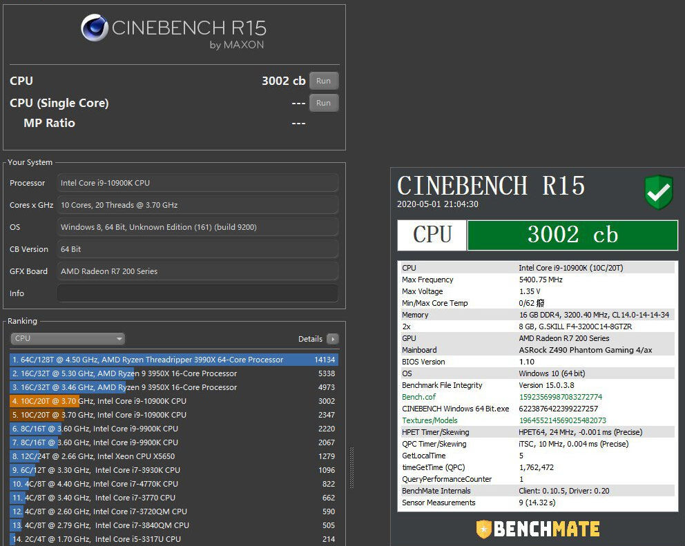
A PC enthusiast on ChipHell, with access to an i5-10400, tested it on an MSI MAG Z490 Tomahawk motherboard, and compared its performance with the i5-9400F. Among the strictly-synthetic tests are Cinebench R15 and R20, various forms of CPU-Z bench, and SuperPi. The processor posts a tiny 2-5% performance gain in single-threaded tests that scale perfectly with its 4.8% higher max boost frequency (4.30 GHz vs. 4.10 GHz on the i5-9400F). It's the multi-threaded tests where the i5-10400 comes alive, thanks to HyperThreading. It posts massive 35-45% performance gains with CPU-Z bench multi-threaded; a 41.85% gain with Cinebench R20 nT, and 45.05% gain with Cinebench R15 nT. This would bring the i5-10400 within 10-15% of the Ryzen 5 3600X in multi-threaded Cinebench tests.
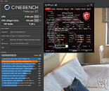

A PC enthusiast on ChipHell, with access to an i5-10400, tested it on an MSI MAG Z490 Tomahawk motherboard, and compared its performance with the i5-9400F. Among the strictly-synthetic tests are Cinebench R15 and R20, various forms of CPU-Z bench, and SuperPi. The processor posts a tiny 2-5% performance gain in single-threaded tests that scale perfectly with its 4.8% higher max boost frequency (4.30 GHz vs. 4.10 GHz on the i5-9400F). It's the multi-threaded tests where the i5-10400 comes alive, thanks to HyperThreading. It posts massive 35-45% performance gains with CPU-Z bench multi-threaded; a 41.85% gain with Cinebench R20 nT, and 45.05% gain with Cinebench R15 nT. This would bring the i5-10400 within 10-15% of the Ryzen 5 3600X in multi-threaded Cinebench tests.