Wednesday, July 27th 2011

Intel Aims at 10 nm Processors by 2018
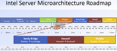
It's not just host nations of the Olympics that are decided almost decades in advance, but also Intel's silicon names and the fab process they're going to be built on. Intel has its plan for the greater part of this decade already charted out, well beyond the upcoming Ivy Bridge architecture. Intel follows the "tick-tock" product cycle, where every micro-architecture gets to be built on two succeeding fab processes, and every fab process getting to have two succeeding micro-architectures built on it, in succession. Westmere is an optical shrink of the Nehalem architecture, it was a "tick" for the 32 nm process, Sandy Bridge is its "tock", and a new architecture. Ivy Bridge is essentially an optical shrink of Sandy Bridge, it is the "tick" for 22 nm process.
Ivy Bridge will make its entry through the LGA1155 platform in 2012, it will make up the 2012 Core processor family. Haswell is the next-generation architecture that succeeds Sandy Bridge and IvyBridge, it will be built on the 22 nm process, and is expected to arrive in 2013. Roswell is its optical shrink to 14 nm, slated for 2014. Looking deep into the decade, there's Skylake architecture, that will span across 14 nm and 10 nm processes with Skymont. This model ensures that Intel has to upgrade its fabs every 2 or so years, an entirely new micro-architecture every 2 or so years as well, while providing optical shrinks every alternating year. Optical shrinks introduce new features, increased caches, and allow higher clock speeds. 10 nm for processors by 2018 sounds realistic looking at the advancement of NAND flash technologies that are pushing the boundaries of fab process development. NAND flash is much less complex than processor development, and hence serve as good precursors to a new process.
Source:
ComputerBase.de
Ivy Bridge will make its entry through the LGA1155 platform in 2012, it will make up the 2012 Core processor family. Haswell is the next-generation architecture that succeeds Sandy Bridge and IvyBridge, it will be built on the 22 nm process, and is expected to arrive in 2013. Roswell is its optical shrink to 14 nm, slated for 2014. Looking deep into the decade, there's Skylake architecture, that will span across 14 nm and 10 nm processes with Skymont. This model ensures that Intel has to upgrade its fabs every 2 or so years, an entirely new micro-architecture every 2 or so years as well, while providing optical shrinks every alternating year. Optical shrinks introduce new features, increased caches, and allow higher clock speeds. 10 nm for processors by 2018 sounds realistic looking at the advancement of NAND flash technologies that are pushing the boundaries of fab process development. NAND flash is much less complex than processor development, and hence serve as good precursors to a new process.

64 Comments on Intel Aims at 10 nm Processors by 2018
Intel is not stupid. They do not base their production futures off of hopeful numbers, they base them off of reality.
When light transfer methods (for resist etching) could no longer work they had developed doping. When traditional silicon didn't provide enough resistance they developed high-k gate materials. When 2d transistors posed heat dissipation issues they developed 3d transistors. As high-k materials are becoming insufficient they are researching graphene solutions.
Now spend a little time thinking about the manufacturing environment. Research needs to be completed, prototypes need to be made, production machinery needs to be designed, machinery needs to be fabricated and installed, trial runs need to be made, and the people need to be trained for production. Two years to do all of this means that, right now, Intel is very likely testing the basic prototypes of the 10 nm process. If not, they can't be far off.
Current problems with the 22 nm process are very likely to not make any difference in the future plans. Scaling the process for production is a different challenge than research. Whenever you understand how a machine like Intel works, you understand that one delay doesn't have the same domino effect that it would at other companies.
My 960 should get me by till then.
Intel arms Haswell with DX11.1
www.sweclockers.com/nyhet/14288-intel-ger-stod-for-directx-111-i-haswell