Tuesday, September 26th 2017

AMD Zen 2 Architecture: Socket AM4, 2019, Code-named "Matisse"
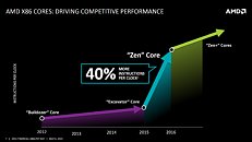
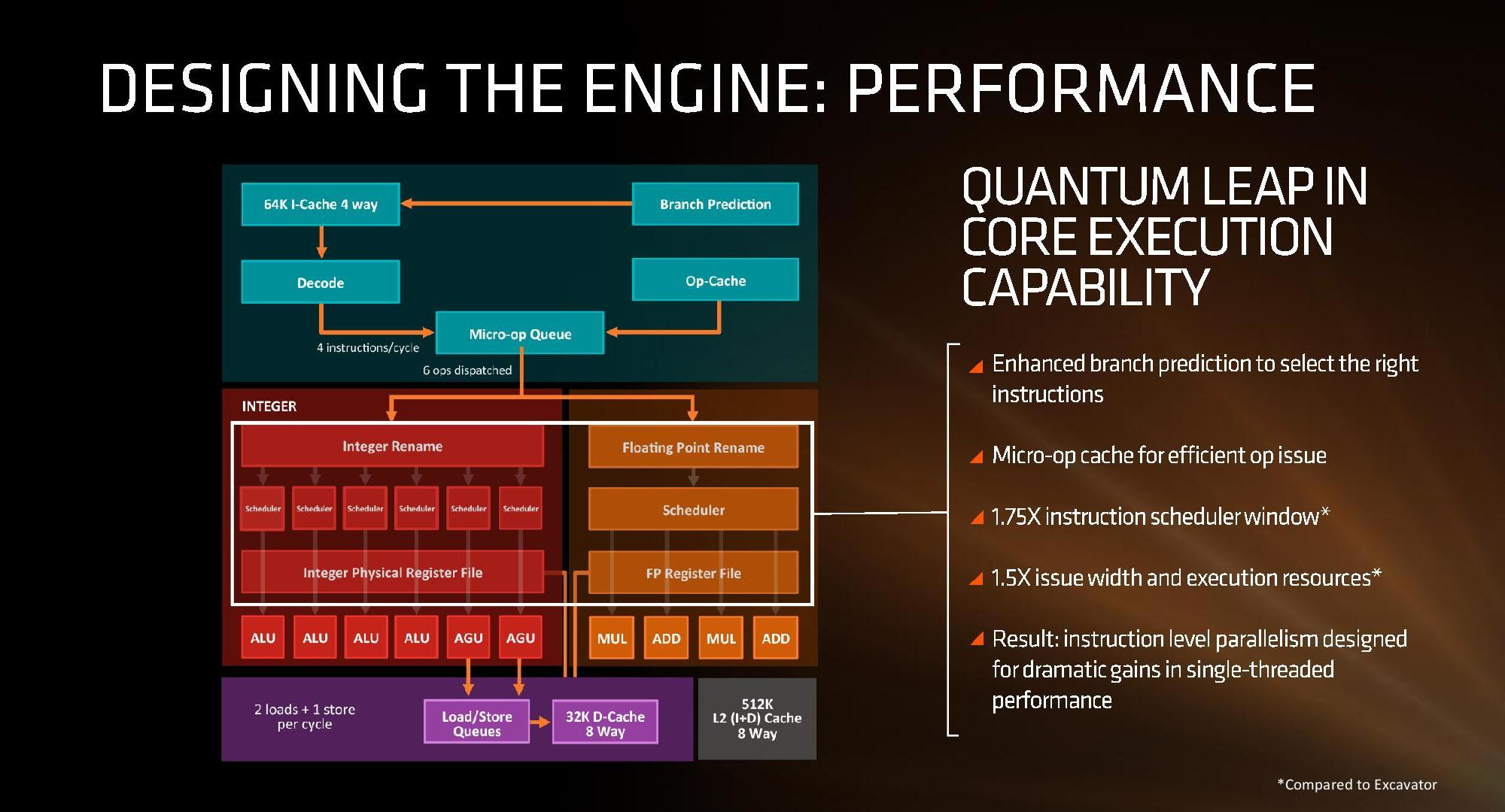
AMD's Zen-based Ryzen and Threadripper have been said by the company as representing the "worst case scenario" of performance for their architecture. This is based on the fact that there are clear areas for improvement that AMD's engineers were keenly aware of even at the moment of Zen's tapping-out; inadvertently, some features or improvements were left on the chopping block due to time and budget constraints. As unfortunate as this is - who wouldn't love to have even more performance on their AMD processors - this also means AMD has a clear starting point in terms of improving performance of their Zen micro-architecture.
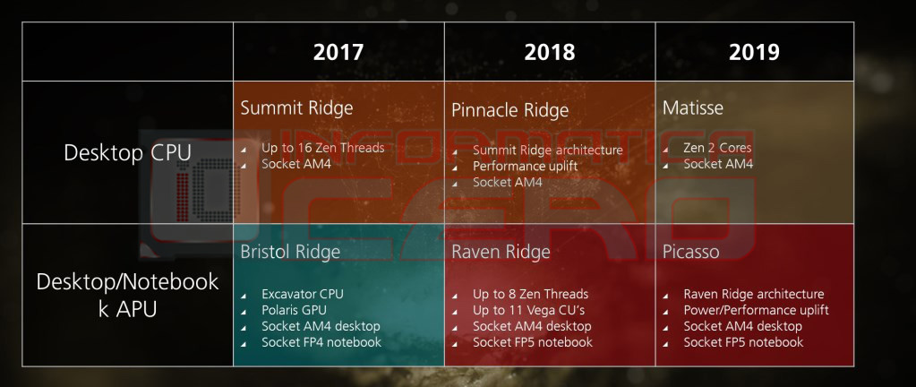
Spanish website Informatica Cero have gotten their hands on what they say is an exclusive, real piece of information from inside AMD, which shows the company's CPU roadmap until 2019, bringing some new details with it. On the desktop side, there's mention of AMD's "Pinacle Ridge" as succeeding the current Zen-based "Summit Ridge" Ryzen CPUs in 2018. These leverage the same Summit Ridge architecture, but with a performance uplift; this plays well into those reports of 12 nm being used to manufacture the second-generation Ryzen: it's an AMD tick, so to say. As such, the performance uplift likely comes from increased frequencies at the same power envelope, due to 12 nm's denser manufacturing design.

 Another interesting tidbit from this slide is the confirmation of AMD's Zen 2 processors being released in 2019. Based on the company's revised Zen 2 cores (which should see those architectural improvements we were talking about in the beginning of this piece), AMD also seems to be doing away with the ridge-like codenames they've been using in recent times, and taking a more artistic approach. Matisse seems to be the code-name for AMD's Zen 2 architecture, and if you know your painters, it looks like AMD is betting on its Zen 2 cores to further define and influence CPU design. There is no mention of increased Zen threads, however, which likely points towards AMD keeping the same 8-core, 16-thread design as with their current Summit Ridge. This likely plays into AMD's plan for keeping the AM4 socket relevant - while good for consumers who might want to see longevity in their platform, it does prevent AMD from making more radical design changes to their architecture.
 Jumping towards its notebook/desktop APU designs, AMD is looking to accompany Matisse with their code-named Picasso APUs for 2019. These should still leverage the company's upcoming Raven Ridge line of APUs, which pair Vega 11 NCUs on the graphical side of the equation and up to 8 Zen threads (4-core CPUs with SMT). However, usage of 12 nm processes across both its Zen CPU cores and Vega 11 NCUs apparently give AMD confidence that they can improve Picasso over Raven Ridge not only in the performance fields, but also the power consumption metrics.
A little bit of lore: AMD seems to be changing their code-names towards painters, and the marriage of Matisse in the CPU and Picasso in the APU space isn't a coincidence. Both artists are considered two of the most important players in the arts space of the beginning of the twentieth century, responsible for both defining and developing the arts. AMD's choice of both of them is, therefore, not a fluke; it's likely more of an artistic take on the company's vision of further defining itself as a key innovative player in the CPU space.

Sources:
Informatica Cero, Pablo Picasso @ Wikipedia, Henri Matisse @ Wikipedia
Spanish website Informatica Cero have gotten their hands on what they say is an exclusive, real piece of information from inside AMD, which shows the company's CPU roadmap until 2019, bringing some new details with it. On the desktop side, there's mention of AMD's "Pinacle Ridge" as succeeding the current Zen-based "Summit Ridge" Ryzen CPUs in 2018. These leverage the same Summit Ridge architecture, but with a performance uplift; this plays well into those reports of 12 nm being used to manufacture the second-generation Ryzen: it's an AMD tick, so to say. As such, the performance uplift likely comes from increased frequencies at the same power envelope, due to 12 nm's denser manufacturing design.


A little bit of lore: AMD seems to be changing their code-names towards painters, and the marriage of Matisse in the CPU and Picasso in the APU space isn't a coincidence. Both artists are considered two of the most important players in the arts space of the beginning of the twentieth century, responsible for both defining and developing the arts. AMD's choice of both of them is, therefore, not a fluke; it's likely more of an artistic take on the company's vision of further defining itself as a key innovative player in the CPU space.

65 Comments on AMD Zen 2 Architecture: Socket AM4, 2019, Code-named "Matisse"
If they can keep this up, it's gonna make PC great again
a 8700K is becoming less and less desirable for me, hell even the 8600K is loosing his appeal in favor of a R5 1600/1600X (or R7 if i had the mean to take a 8700K instead of a 8600K) .... even with the actual clock speed and meager OC potential
since the Zen 2 will be also on AM4 ...
but will it need a new chipset? probably not, will it be retro compatible? probably ... we are not talking about Intel in this case ...
the last good point of Intel, is their set of blind follower that will buy my 6600K+Z170G7+16gb 2800 literally near the initial launch price .... (did some search checked some similar offers ... i could buy a full set in AM4 CPU/Mobo + compatible RAM and still have ~200chf if taking a R5 or ~100-145chf if taking a R7 :laugh: )"close minded blind follower" is the keyword :laugh: (joke)
Its interesting that automotive is mentioned ,but on 12nmlpp similar but slightly conflicting, SOI on zen would push the price up and allow higher clocks but the cost rises too so im thinking this 12nm is all the goodies in the 14nm hpe minus the SOi.
Anyway good times ahead ,both big x86 players are really in the game.
As the previous poster pointed out, sure GloFo could do higher clocks, but it would eliminate the power advantage ryzen has, not to mention make the mobile market a hopeless endeavor AGAIN. I would ratherAMD continue improving IPC rather then getting into another disastrous clockspeed war.
The z14 along with the SPARC M8 are the only high end processors that can do 5GHz 24x7 & that has to count as some sort of achievement, considering the Intel advantage wrt x86 & their own foundries.
FX CPUs did 5 Ghz easily too , on a node that is what , half a decade old ? It's all down to the node and architecture. How many pipeline stages it features , how wide the instructions are , how much cache there is and how fast it runs. There are so many things that affect clock speed besides the manufacturing process.
The fact that GF can make 5Ghz chips on their newest nodes doesn't tell us anything with regards to Zen+ or Zen 2. Can those do 5 Ghz on that node ? No way to tell , it's all 100% guesses at this point.
And it's not even entirely about technical capabilites , maybe GF and AMD can make these chips run at 5 ghz+ , but is it cost effective ? Those IBM CPUs must cost a fortune.
The contradiction on forums is getting ridiculous, who mentioned mobile, not me im talking Hpc and how do you improve Ipc without arch changes on mass without frequency going up.
It's ok for intel to pr blurb 4.8ghz ocs with 5ghz via delid for its new coffee lake but Amd better not try for higher clocks too because you won't like it.
Do you not read,,,, that 8800k at 5ghz is not going to be power efficient.
Shit check the recent I9 world record , 1000watts plus through an Intel cpu.
Physics are what they are and intel play with the same rulebook.
. and all decrying 14nmhpe irrelevant because its used for mainframes, its not just for mainframes its a foundry node you could easily make x86 on it, they aren't and i started this by saying they could but are not.
But they could be using some of its pdk improvement recipe points on its 12nm lpp as to me that's whats implied by separate news items rumour and a bit of smoke.