Thursday, January 5th 2023

AMD Shows Instinct MI300 Exascale APU with 146 Billion Transistors

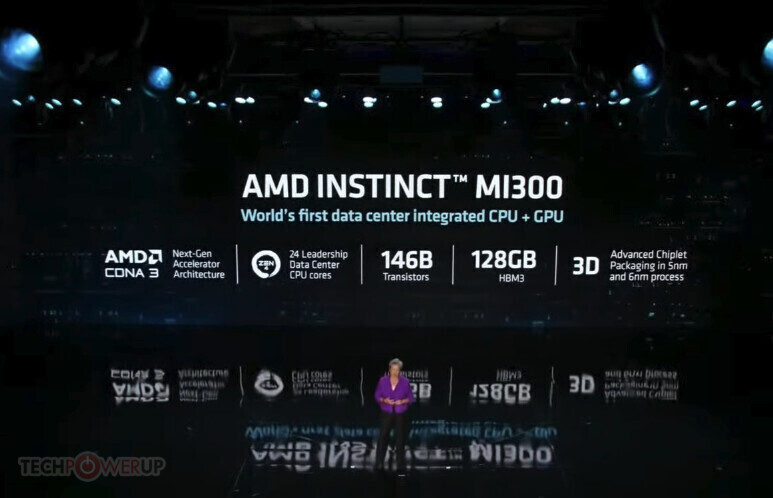
During its CES 2023 keynote, AMD announced its latest Instinct MI300 APU, a first of its kind in the data center world. Combining the CPU, GPU, and memory elements into a single package eliminates latency imposed by long travel distances of data from CPU to memory and from CPU to GPU throughout the PCIe connector. In addition to solving some latency issues, less power is needed to move the data and provide greater efficiency. The Instinct MI300 features 24 Zen4 cores with simultaneous multi-threading enabled, CDNA3 GPU IP, and 128 GB of HBM3 memory on a single package. The memory bus is 8192-bit wide, providing unified memory access for CPU and GPU cores. CLX 3.0 is also supported, making cache-coherent interconnecting a reality.

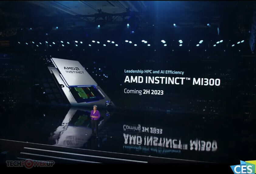
The Instinct MI300 APU package is an engineering marvel of its own, with advanced chiplet techniques used. AMD managed to do 3D stacking and has nine 5 nm logic chiplets that are 3D stacked on top of four 6 nm chiplets with HBM surrounding it. All of this makes the transistor count go up to 146 billion, representing the sheer complexity of a such design. For performance figures, AMD provided a comparison to Instinct MI250X GPU. In raw AI performance, the MI300 features an 8x improvement over MI250X, while the performance-per-watt is "reduced" to a 5x increase. While we do not know what benchmark applications were used, there is a probability that some standard benchmarks like MLPerf were used. For availability, AMD targets the end of 2023, when the "El Capitan" exascale supercomputer will arrive using these Instinct MI300 APU accelerators. Pricing is unknown and will be unveiled to enterprise customers first around launch.
Add your own comment

44 Comments on AMD Shows Instinct MI300 Exascale APU with 146 Billion Transistors

#26
AnotherReader
WirkoImpressive, and I hope we soon learn more about how it's structured. Three Zen CCDs plus multiple GPU dies on top, among other chips, apparently. Four cache+MC dies beneath, but those can't be nearly as big as the nine on top. (?) But why didn't AMD choose to place the cache+MC dies under HBM stacks?

And ... This thing will also require 3D power delivery electronics all around.
Placing the cache die under the compute dies would minimize added latency as can be seen in the case of the 5800X3D. It will probably allow better cooling too as the compute dies are the power hogs. Moreover, as you said, I expect that the MCDs would have much more wiring for power than the MCDs for the consumer RDNA3 GPUs.
Posted on Reply
#27
TheoneandonlyMrK
ARFI don't work with nvidia :D
I said AMD is to blame because most of the time it doesn't deliver up to the expectations. The users want the fastest. AMD never delivers the fastest.
Actually, if RDNA 1 and before Vega 64, etc garbage, they simply ignored the top of the line market - the halo which sells the whole product lineup beneath it.

:D


Exactly. AMD must concentrate on working relationships with those "OEM"s.
Or build its own ecosystem without them - direct sales, etc.
That's AMD to blame - because nvidia and Intel concentrate on buying the "OEM", so the result which you see in the stores is 99% Intel-nvidia exclusives.
People see only what they Want to see, I see plenty of alternatives to Nvidia and Intel and my five year old and still better than the 1080 non ti Vega64, it was released against says you're wrong, but more importantly, this isn't a GPU thread FFS.

Shall we discuss the XTX overhaet issue next, how about we leave DGPU talk to threads that suit it?!.

Not Enterprise which is showing up your naivety.
Posted on Reply
#28
Leiesoldat
lazy gamer & woodworker
Nexus290
Vya DomusIntel has a similar solution with Ponte Vecchio, which
LeiesoldatPonte Vecchio is inside the Aurora supercomputer which is still on track, albeit slowly.
Aurora was first announced in 2015 and to be finished in 2018.
Yes they said Aurora was going to be finished in 2018, but Intel kept tacking on more and more capability to match Frontier which pushed the scheduled completion date out. Aurora being delayed is not a secret to anybody in the HPC industry, but the likely completion date is going to be somewhere between now and a maybe 2024; Intel keeps those dates hidden.
Posted on Reply
#29
ADB1979
AnotherReaderPlacing the cache die under the compute dies would minimize added latency as can be seen in the case of the 5800X3D. It will probably allow better cooling too as the compute dies are the power hogs. Moreover, as you said, I expect that the MCDs would have much more wiring for power than the MCDs for the consumer RDNA3 GPUs.
The added cache is on top of the die because routing through it would be a nightmare if it was underneath, that is the primary reason why the cache is on the top.

The 3D-V Cache power use, plus heat from the silicon below doesn't make a lot of difference to temperature because of how it is manufactured, plus the die selection that has been made, plus the 3D-V Cache has been designed to sit directly over the CPU Cache, it cant just be placed anywhere, and so any other products AMD wants to make where they can stack 3D-V Cache has to be designed that way from the start, and the 3D-V Cache has to be designed to fit the die below it, such as the MCD's on their new GPU's, are they the same as for the Zen CPU's.? I doubt it.

As for the latency point, I don't see how it would reduce latency by having the 3D-V Cache on the underside of the CPU die, if anything I think that apart from being a wiring nightmare, it would add latency as the processor die would be just a little further away from the substrate, and thus everything that it is communicating with, RAM, and I/O I imagine the difference of a few microns would be minimal, and if so, it would also be minimal if the cache was underneath the compute dies ¯\_(ツ)_/¯
Posted on Reply
#30
AnotherReader
ADB1979As for the latency point, I don't see how it would reduce latency by having the 3D-V Cache on the underside of the CPU die, if anything I think that apart from being a wiring nightmare, it would add latency as the processor die would be just a little further away from the substrate, and thus everything that it is communicating with, RAM, and I/O I imagine the difference of a few microns would be minimal, and if so, it would also be minimal if the cache was underneath the compute dies ¯\_(ツ)_/¯
As you said, there are good reasons for the cache die being on top of the CPU die. Let's see what they are doing with this one. However, the cache die is much smaller than the CPU die, and making it large enough to devote area to power wiring might solve the power delivery issues. If the latency impact of off-chip access was insignificant, the 5800X3D wouldn't have had the cache placed on top of the main die.
Posted on Reply
#31
Wirko
AnotherReaderAs you said, there are good reasons for the cache die being on top of the CPU die. Let's see what they are doing with this one. However, the cache die is much smaller than the CPU die, and making it large enough to devote area to power wiring might solve the power delivery issues. If the latency impact of off-chip access was insignificant, the 5800X3D wouldn't have had the cache placed on top of the main die.
Tom's has a few photos. Four large dies are visible on top ... and that still doesn't explain anything.
Posted on Reply
#32
TumbleGeorge
Strange in TPU GPU database all numbers, include those for performance for MI250X and MI300 are same.
Posted on Reply
#33
JAB Creations
terroralphaas an AMD shareholder, i'm so glad they don't listen to random people on the internet.
Please, visit every AMD related news article, wait for the first 3-4 fools to post and just reply with this. :toast:
Posted on Reply
#34
mkppo
ARFThere is also 10 times more money in the graphics market ! 8% today market share with outlook for probable bankruptcy, or 80% market share as is case with nvidia !
You sound like a child with these silly statements. I see you have a pattern for dissing AMD wherever you can but atleast be clever about it. AMD gets around 10x the money for every instinct they sell compared to desktop GPU's. Also, probably bankruptcy? They had 1 billion in profits in 2022, which would've been double had they not written off a bunch of money after Xilinx acquisition. They shrank much lower than your beloved intel and nvidia. They care about margins and profits, like every large company, and that's exactly where they are focusing their R&D. The MI300 is an absolutely staggering achievement, just the sheer complexity is mind boggling.
So, please answer me. What possible bankruptcy? Be clever with your response please, get out of the 10 year old mindset and subsequent comments.
Posted on Reply
#35
The Von Matrices
8x performance improvement and 5x efficiency improvement?

That's a very clever way of disguising a 60% increased TDP.
Posted on Reply
#36
terroralpha
The Von Matrices8x performance improvement and 5x efficiency improvement?

That's a very clever way of disguising a 60% increased TDP.
TDP doesn't matter. what matters is density and efficiency.
JAB CreationsPlease, visit every AMD related news article, wait for the first 3-4 fools to post and just reply with this. :toast:
sometimes the things i read make me cringe so hard i scramble to close the browser tab. some posts are so bad that i don't even know how to reply. i don't even know where to start. so i don't.
Posted on Reply
#37
Patriot
LeiesoldatPonte Vecchio is inside the Aurora supercomputer which is still on track, albeit slowly.
Making progress is different than on track.
Aurora was first announced in 2015 and to be finished in 2018
2017, delayed to 2021 but scaled up to 1 exaFLOP (with Ponte Viecchio)
October 2020, delayed another 6mo.
October 2021, Intel took a 400m Loss on the checkbook and Aurora is targeted for 2023 and 2exaflops.
The Von Matrices8x performance improvement and 5x efficiency improvement?

That's a very clever way of disguising a 60% increased TDP.
I am curious to see AMD's reply as to how this chip works in multi configs...
It looks... like its 2 socket max. It looks like a 4 GPU chiplet with 4x8 zen4 chiplets betwen the hbm stacks.
Taking node from 4x 560w to 2x idk 700-900w? Unclear if it will need a parent cpu, as each APU has 96 Zen4 cores onboard.
Also the block diagram is notably different than the chip in hand and pictured.

For all of you (ARF) that clearly missed it, AMD was very proudly showing off their insanely profitable Xilinx wing, under the new AMD XDNA branding.
That new FPGA Decimates the inference card by nvidia in the same class... AMD is taking advantage of NVidia abandoning the 75w slot.
www.xilinx.com/content/dam/xilinx/publications/product-briefs/alveo-v70-product-brief.pdf
Nvidia replaced the T4 with the A2 and it's barely better. www.nvidia.com/en-us/data-center/tesla-t4/ www.nvidia.com/en-us/data-center/products/a2/
Left room for AMD.
Posted on Reply
#38
mrnagant
ARFInstead of focusing on already super developed market segments which do not need so much attention, better AMD focus on the discrete graphics business. Very very lame !
That is where the money is. Read financial reports. Takes only a few minutes. AMD in Q3 2022 revenue of $1.6B datacenter segment, $1.6B gaming segment, $1B client segment. 30% margins from datacenter, 10% from gaming and slight negative on the client. AMD also has higher yoy increases on datacenter.

There is more growth oppertunity with higher returns in datacenter.

Look at Nvidia. Q3 2022 they pulled in $3.8B datacenter, up 31% yoy and gaming was $1.6B, down 51% yoy. Looking at Nvidia's stack, it is geared for datacenter. Even watching Nvidia's release of gaming GPUs, there is way more focus on everything outside gaming. But gaming gets to benefit from a lot of these features that they primarily are selling for enterprise.
Posted on Reply
#39
Solaris17
Super Dainty Moderator
This gives me Xeon Phi vibes with the added GPU element.
Posted on Reply
#40
kapone32
MysteoaYou are talking about Gaming GPUs market, which doesn't bring as much money as the server space and professional. Just look at Nvidia selling the same gaming gpu die to professionals or server for 10x the price.

Nvidia makes 58% of it revenue from Compute & Networking and 42% from Graphics. Graphics include Gaming GPU and streaming, professional Quadro/RTX GPUs and Visualization software, Automotive. So if we remove the non gaming stuff, the revenue just from Gaming is even less, it's about 26% from NVidia Q3 2022 Financial Results. Why would AMD aim for a market that brings only 26% of NVIDIA revenue when it can go for the bigger one?
You forgot Mining you cannot use Nvidia without incorporating Mining in 2021 you could buy a 30 series card retail but Thousands of Mining farms using 3070s and 3080s or do we forget that they released a driver nerfing mining on those cards?
Posted on Reply
#41
TumbleGeorge
Solaris17This gives me Xeon Phi vibes with the added GPU element.
But just some hundred times faster?
Posted on Reply
#42
kapone32
This is an astounding technical achievement.
Posted on Reply
#43
Solaris17
Super Dainty Moderator
TumbleGeorgeBut just some hundred times faster?
I would hope so Phi is super old. You wouldnt compare this directly to old accelerator cards from Intel or anyone else.
Posted on Reply
#44
TumbleGeorge
Solaris17I would hope so Phi is super old. You wouldnt compare this directly to old accelerator cards from Intel or anyone else.
Of course, the Intel product you mentioned was never very successful and widespread. I wouldn't kidding with the dead.
Posted on Reply
Add your own comment
Dec 19th, 2024 09:58 EST change timezone

New Forum Posts

Popular Reviews

Controversial News Posts