News Posts matching #10 nm

Return to Keyword Browsing

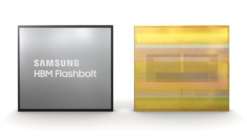
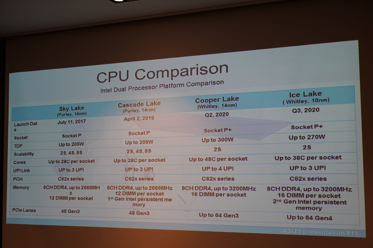
Samsung Launches 3rd-Generation "Flashbolt" HBM2E Memory

Samsung Electronics, the world leader in advanced memory technology, today announced the market launch of 'Flashbolt', its third-generation High Bandwidth Memory 2E (HBM2E). The new 16-gigabyte (GB) HBM2E is uniquely suited to maximize high performance computing (HPC) systems and help system manufacturers to advance their supercomputers, AI-driven data analytics and state-of-the-art graphics systems in a timely manner.

"With the introduction of the highest performing DRAM available today, we are taking a critical step to enhance our role as the leading innovator in the fast-growing premium memory market," said Cheol Choi, executive vice president of Memory Sales & Marketing at Samsung Electronics. "Samsung will continue to deliver on its commitment to bring truly differentiated solutions as we reinforce our edge in the global memory marketplace."

Intel Core i5-L16G7 is the first "Lakefield" SKU Appearance, Possible Prelude to New Nomenclature?

Intel Core i5-L16G7 is the first commercial SKU that implements Intel's "Lakefield" heterogenous x86 processor architecture. This 5-core chip features one high-performance "Sunny Cove" CPU core, and four smaller "Tremont" low-power cores, with an intelligent scheduler balancing workloads between the two core types. This is essentially similar to ARM big.LITTLE. The idea being that the device idles most of the time, when lower-powered CPU cores can hold the fort; performance cores kick in only when really needed, until which time they remain power-gated. Thai PC enthusiast TUM_APISAK discovered the first public appearance of the i5-L16G7 in an unreleased Samsung device that has the Userbenchmark device ID string "SAMSUNG_NP_767XCL."

Clock speeds of the processor are listed as "1.40 GHz base, with 1.75 GHz turbo," but it's possible that the two core types have different clock-speed bands, just like the cores on big.LITTLE SoCs. Other key components of "Lakefield" include an iGPU based on the Gen11 graphics architecture, and an LPDDR4X memory controller. "Lakefield" implements Foveros packaging, in which high-density component dies based on newer silicon fabrication nodes are integrated with silicon interposers based on older fabrication processes, which facilitate microscopic high-density wiring between the dies. In case of "Lakefield," the Foveros package features a 10 nm "compute field" die sitting atop a 22 nm "base field" interposer.

Intel Reportedly Looking Into Further Reduction in CPU Pricing for 2020

Intel's policy on CPU pricing has been a strong, definite one for years: no price reductions. Faced with less than admirable competition from a struggling AMD back in its Phenom and especially Bulldozer days, Intel enforced a heavy hand on the market and on CPU pricing. However, a much revitalized AMD and difficulties in the transition to the 10 nm process have left Intel with no other recourse than to cut pricing on its CPUs in order to remain competitive. No uptake of new I/O technologies such as PCIe 4.0 has also taken its toll on Intel's position in the server and HEDT market, which has led to recent price-cuts and tightening of Intel's Xeon line of CPUs - as well as price-cuts in the order of 50% in their Cascade Lake-X processors compared to the previous generation.

DigiTimes, citing industry PC makers, says that Intel is gearing up to keep fighting in the only front it actually can, besides puny core count increases on their heavily-iterated Skylake architecture - pricing. This move comes in a bid to keep its market dominance, which Intel themselves have said - after Zen 2, that is - isn't a priority for the consumer market. You can rest assured that Intel is very, very likely already practicing hefty price reductions for tray-quantity purchases for partners. However, it seems that the company might bring some price cuts on to its upcoming Comet Lake CPUs. The company has always been loathe to reduce pricing on existing inventory, rather choosing to reduce the price on new launches (see the Cascade Lake-X example above), which, arguably, saves Intel's face on claims of only being able to compete on pricing - which lurks dangerously close to Intel being painted as the budget, price-cut alternative to AMD.

Intel "Panther Canyon" NUC Implements "Tiger Lake" SoC with Xe Graphics

Intel NUC 11 Extreme is the spiritual successor to the "Hades Canyon" and "Skull Canyon" NUC, and implements the company's next-generation 10 nm+ "Tiger Lake" processor. Codenamed "Panther Canyon," the NUC 11 Extreme represents a line of ultra-compact desktops with serious computing power, bringing together the company's highest-performance CPU cores and iGPUs. The "Tiger Lake-U" SoC powering the NUC 11 Extreme will reportedly be configured with a 28-Watt TDP, and will come in Core i3, Core i5, and Core i7 variants.

The "Tiger Lake-U" processor is expected to combine next-generation "Willow Cove" CPU cores with an iGPU based on Intel's new Xe graphics architecture, in what could be the first commercial outing for both. The NUC 11 Extreme "Panther Canyon" will also support up to 64 GB of dual-channel DDR4-3200 memory over SO-DIMMs, an M.2-2280 slot with PCI-Express 4.0 x4 and SATA 6 Gbps wiring, and option for Intel Optane M10 cache memory. On the connectivity front, and Intel AX-201 WLAN card provides 802.11ax Wi-Fi 6, and Bluetooth 5. A 2.5 GbE wired interface will also be available. These will also be among the first NUCs to feature front- and rear-Thunderbolt ports (possibly next-gen 80 Gbps given that the platform implements PCIe gen 4.0). The NUC 11 Extreme "Panther Canyon" is expected to launch some time in the second half of 2020.

Intel CPU Based on New Architecture Leaks

Today Intel's CPU based on yet unannounced architecture got revealed in the SiSoft benchmark database. Featuring six cores and twelve threads running at 3 GHz, it appears like a regular 14 nm CPU that's already available, however, when digging through the details, many things are revealed. The newly submitted CPU has a different L2 cache configuration from previous CPU offerings, with this chip featuring 1.25 MB of L2 cache per core, it is unlike anything else Intel currently offers. Ice Lake mobile chips feature 512 KB, while the highest amount of L2 cache is currently present on i9-10980XE, which features 1 MB of L2.

It is unknown where this CPU fits in the whole 14/10 nm lineup, as we don't know if this is an iteration of 10 nm Tiger Lake or the rumored 14 nm Rocket Lake CPU. All we know is that this CPU features new architecture compared to Skylake iterations that are currently being used, judging by L2 cache bump, which usually happens on new architectures. The platform used for benchmarking this CPU was SuperMicro X12DAi-N SMC X12 dual-socket motherboard, which featured two of these new CPUs for a total of 12 cores and 24 threads.

Intel "Rocket Lake" an Adaptation of "Willow Cove" CPU Cores on 14nm?

The "Willow Cove" CPU core design succeeds "Sunny Cove," Intel's first truly new CPU core design in close to 5 years. "Sunny Cove" is implemented in the 10 nm "Ice Lake" microarchitecture, and "Willow Cove" cores are expected to debut with the 10 nm+ "Tiger Lake." It turns out that Intel is working to adapt "Willow Cove" CPU cores onto a 14 nm microarchitecture, and "Rocket Lake" could be it.

Twitter user @chiakokhua, a retired VLSI engineer with high hit-rate on CPU microarchitecture news, made sense of technical documents to point out that "Rocket Lake" is essentially a 14 nm adaptation of "Tiger Lake," but with the iGPU shrunk significantly, to make room for the larger CPU cores. The Gen12 iGPU on "Rocket Lake-S" will feature just 32 execution units (EUs), whilst on "Tiger Lake," it has three times the muscle, with 96 EUs. "Rocket Lake" also replaces "Tiger Lake's" FIVR (fully-integrated voltage regulation) with a conventional SVID VRM architecture.

Samsung Scores PC CPU Manufacturing Order from Intel

Samsung has reportedly secured a "PC CPU" manufacturing order from Intel. This would entail Intel using Samsung's fabs to manufacture its processors. "PC CPU" is a broad term, interchangeable with "client CPU," and could include both notebook and desktop processors, spanning the "S," "H," "U," and "Y" silicon variants (mainstream desktop, mainstream notebook, ultrabook, and ultra low-power, respectively). Samsung's bouquet of contract-manufacturing covers not just silicon fabrication across 14 nm, but also sub 10 nm nodes, but also provides other key stages of processor manufacturing, including bumping and packaging. Intel would want minimal expenditure in adapting its chip designs to Samsung's nodes

In her November 20 letter addressed to Intel's customers, executive V-P and GM for sales, marketing, and communications, Michelle Johnston Holthaus, mentioned that in addition to Intel's own manufacturing facilities, the company is roping in "foundries" (third-party silicon fabrication companies) to meet demand. Samsung and TSMC lead the foundry business, followed by the likes of GlobalFoundries, UMC, etc.
Many Thanks to biffzinker for the tip.

Intel "Rocket Lake-S" Desktop Processor Comes in Core Counts Up to 8, Gen12 iGPU Included

Intel's 11th generation Core "Rocket Lake-S" desktop processor will come in core-counts only up to 8, even as its predecessor, "Comet Lake-S," goes up to 10. Platform descriptors for Intel's next four microarchitectures surfaced on the web, detailing maximum values of their "S" (mainsteam desktop), "H" (mainstream notebook), "U" (ultrabook), and "Y" (low power portable) flavors. Both "Comet Lake-S" and "Rocket Lake-S" are 14 nm chips. "Comet Lake-S" comes with core counts of up to 10, a TDP of up to 125 Watts, Gen 9LP iGPU with 48 execution units, and native support for up to 128 GB of DDR4-2667.

The "Rocket Lake-S" silicon is interesting. Rumored to be yet another derivative of "Skylake," it features up to 8 CPU cores, the same 125 W maximum TDP, but swanky Gen12 iGPU with 32 execution units. The memory controller is also upgraded, which supports DDR4-2933 natively. There is no "Ice Lake-H" or "Ice Lake-S" in sight (no mainstream notebook or mainstream desktop implementations), ditto "Tiger Lake." For the foreseeable future, Intel will only make quad-core designs of the two 10 nm microarchitectures. "Rocket Lake-S" is slated for 2021 when, hopefully, we'll see Intel escape the 14 nm black hole.

Dell Calls Out Intel for CPU Shortages Affecting its 2019 Full Year Revenue Forecast

PC major Dell in its quarterly results call blamed Intel for cuts in its revenue forecast for 2019 (full year) sales. "Intel CPU shortages have worsened qtr-over-qtr, impacting our commercial PC and premium consumer PC Q4 forecasted shipments," said Dell COO Jeffrey Clarke. Intel's CPU shortages are caused due to demand in the PC and server markets significantly outpacing supply, and not because Intel is supplying below its capacity. The company increased its capex toward manufacturer by $1 billion YoY, retrofitting its manufacturing facilities to make 14 nm processors, all while juggling resources to execute its 10 nm rollout for high-volume mobile and high-margin server processors.

The company hasn't launched 10 nm desktop or HEDT processors, yet, and is reportedly preparing yet another 14 nm line of processors for these platforms, codenamed "Comet Lake." This microarchitecture has also seen a mobile rollout for mainstream mobile form-factors, while Intel focused 10 nm "Ice Lake" for ultraportables and ultra low-power form-factors. Intel executive VP for sales Michelle Johnston Holthaus recently wrote a letter to its customers (primarily companies like Dell,) informing them that despite their best efforts, demand continues to beat supply, and that they hadn't managed to solve their supply issues.

Intel "Tiger Lake" Microarchitecture Features HEDT-like Cache Rebalancing?

With its "Skylake" microarchitecture, Intel significantly re-balanced the cache hierarchy of its HEDT and enterprise multi-core processors to equip CPU cores with larger amounts of faster L2 caches, and lesser amounts on slower shared L3 cache. The company retained its traditional cache balance for its mobile and desktop processor derivatives. This could change with the company's "Tiger Lake" microarchitecture, particularly the "Willow Cove" CPU cores they use, according to a Geekbench online database listing for a prototype quad-core "Tiger Lake-Y" mobile processor.

According to this listing, assuming Geekbench is reading the platform correctly; the "Tiger Lake-Y" processor features a 4-core/8-thread CPU, with a massive 1,280 KB (1.25 MB) of L2 cache per core, and 12 MB of L3 cache. Intel also enlarged the L1D (data) cache to be 48 KB in size, while the L1I (instruction) cache remains 32 KB. This amounts to a 400% increase in L2 cache size, and a 50% increase in L3 cache size. Unlike with "Skylake-X," the increase in L2 cache size doesn't come with a decrease in shared L3 cache size (per core). The "Tiger Lake-Y" processor is being tested on a "Corktown" prototyping platform (a specialized motherboard that has all possible I/O connectivity available with the platform, for testing. "Tiger Lake" is expected to make its debut some time in 2020-21 as a successor to "Ice Lake," and will be built on Intel's refined 10 nm++ silicon fabrication node. Find the Geekbench entry in the source link below.

Intel Announces New GPU Architecture and oneAPI for Unified Software Stack at SC19

At Supercomputing 2019, Intel unveiled its vision for extending its leadership in the convergence of high-performance computing (HPC) and artificial intelligence (AI) with new additions to its data-centric silicon portfolio and an ambitious new software initiative that represents a paradigm shift from today's single-architecture, single-vendor programming models.

Addressing the increasing use of heterogeneous architectures in high-performance computing, Intel expanded on its existing technology portfolio to move, store and process data more effectively by announcing a new category of discrete general-purpose GPUs optimized for AI and HPC convergence. Intel also launched the oneAPI industry initiative to deliver a unified and simplified programming model for application development across heterogenous processing architectures, including CPUs, GPUs, FPGAs and other accelerators. The launch of oneAPI represents millions of Intel engineering hours in software development and marks a game-changing evolution from today's limiting, proprietary programming approaches to an open standards-based model for cross-architecture developer engagement and innovation.

Intel CFO Talks About 7nm Rollout, Delay in 10nm, Increased Competition from AMD

Intel CFO George Davis in an interview with Barron's commented on the company's financial health, and some of the reasons behind its rather conservative gross margin guidance looking forward to at least 2023. Intel's current product stack is moving on to the company's 10 nm silicon fabrication process in a phased manner. The company is allocating 10 nm to mobile processors and enterprise processors, while brazening it out with 14 nm on the client-desktop and HEDT platforms until they can build 10 nm desktop parts. AMD has deployed its high-IPC "Zen 2" microarchitecture on TSMC's 7 nm DUV process, with plans to go EUV in the coming months.

"We're still keenly focused on gross margin. Everything from capital efficiency to the way we're designing our products. What we've said though, the delay in 10 nanometer means that we're going to be a little bit disadvantaged on unit cost for a period of time. We actually gave guidance for gross margin out in 2021 to help people understand. 2023 is the period that we were ultimately guiding [when] we're going to see very strong revenue growth and margin expansion. We've got to get through this period where we have the 10 nanometer being a little bit late [as] we're not optimized on a node that we're on. But [by] then we're moving to a two to two and a half year cadence on the next nodes. So we're pulling in the spending on 7 nanometer, which will start up in the second half of 2021 because we think it's the right thing to do competitively," he said.

Intel Ice Lake-SP and Cooper Lake-SP Details Leaked

Brainbox, a Korean media outlet, has gathered information on Intel's newest Ice Lake and Cooper Lake server processors from a presentation ASUS held for its server lineup. With Cooper Lake-SP paving the way for the first server CPU model to be released on the new "Whitley" platform, it is supposed to launch in Q2 of 2020. Cooper Lake-SP comes with TDP of 300 W and will be available with configurations of up to 48 cores, but there also should be a 56 core model like the Xeon Platinum 9282, that has a TDP of 400 W. Cooper Lake-SP supports up to 64 PCIe 3.0 lanes, 8 channel memory (16 DIMMs in total) that goes up to 3200 MHz and four Ultra Path Interconnect (UPI) links.

Ice Lake-SP, built on the new 10 nm+ manufacturing process, is coming in soon after Cooper Lake-SP release, with a launch window in Q3 of 2020. That is just few months apart from previous CPU launch, so it will be a bit hard to integrate the launches of two rather distinct products. As far as the specifications of Ice Lake-SP goes, it will have up to 38 core for the top end model, within 270 W TDP. It supports 64 PCIe 4.0 lanes with three UPI links. There is also 8 channel memory support, however this time there is an option to use 2nd generation Optane DC Persistent Memory. Both CPU uArches will run on the new LGA 4189 on the P+ socket.

Intel "Tiger Lake-U" Processors Could Support LPDDR5 Memory

Intel's Core "Tiger Lake" microarchitecture could be a point of transition between DDR4 and DDR5 for the company. Prototypes of devices based on the ultra-compact "Tiger Lake-Y" SoC were earlier shown featuring LPDDR4X memory, although a new device, possibly a prototyping platform, in the regulatory queue with the Eurasian Economic Commission describes itself as featuring a "Tiger Lake-U" chip meant for thin and light notebooks and convertibles. This device features newer LPDDR5 memory, according to its regulatory filing.

LPDDR5 succeeds LPDDR4X as the industry's next low-power memory standard, offering data-rates of up to 6,400 MT/s (versus up to 4,266 MT/s of LPDDR4X), and consumes up to 30 percent less power. This prototype at the EEC is sure to be using unreleased LPDDR5 memory chips as DRAM majors Samsung and SK Hynix plan to ship their DDR5-based memory solutions only by the end of this year, although mass-production of the chips have already started at Samsung, in PoP form-factors. A successor to the 10th generation Core "Ice Lake," "Tiger Lake" will be Intel's second CPU microarchitecture designed for its 10 nm silicon fabrication node.

Intel 10 nm Ice Lake is Alive: Server and Desktop Support Added to the Linux Kernel

There were many rumors about Intel's 10 nm CPUs, many of them indicating that Intel will not manufacture 10 nm CPUs for desktop users, due to the 10 nm manufacturing process being in a bad shape. Those rumors were later countered by Intel, claiming that 10 nm is doing very well on improving yields and that we will see desktop CPUs based on the new node very soon.

Thanks to the Linux kernel mailing list (LKML), we now know that support for Ice Lake desktop and server CPUs has been added. A Patch titled "Add more CPU model number for Ice Lake" has many details about variants of Ice Lake with names like Ice Lake X for server Xeon CPU, Ice Lake D for Xeon D CPUs, Ice Lake L for mobile, and regular Ice Lake for desktop series of CPUs. This confirms Intel's claims that Ice Lake is on its way to desktop and server users in the near future. Possible launch date on these CPUs would be sometime in 2020, when Xe graphics cards are launched in July/August, so Intel could bundle both processors on the same 10 nm node.

Intel Could Unveil First Discrete 10 nm GPUs in mid-2020

According to the sources close to DigiTimes, Intel will unveil its first discrete 10 nm graphics cards named "Xe" very soon, with the first wave of Xe GPUs expected to arrive some time in 2020. Said to launch mid year, around July or August, Intel will start selling initial Xe GPU models of the long awaited product to consumers, in hope of gaining a share in the massive market using GPU for acceleration of all kinds of tasks.

Perhaps one of the most interesting notes DigiTimes reported is that "... Intel's GPUs have already received support from the upstream supply chain and has already been integrated into Intel's CPUs to be used in the datacenter and AI fields.", meaning that AIB partners already have access to first 10 nm graphics chips that are ready for system integration. First generation of Xe graphics cards will cover almost whole GPU market, including PC, datacenter, and AI applications where NVIDIA currently holds the top spot.

Intel Clarifies on 10nm Desktop CPUs: Still on the Table, Likely in 2021

Intel in a quick rebuttal to the earlier reports from Monday, clarified that desktop processors based on the 10 nm silicon fabrication node are still on the company's roadmap. "We continue to make great progress on 10 nm, and our current roadmap of 10 nm products includes desktop," the company said in its one-liner. Monday's reports predicted a horror story where Intel would drag its 14 nm "Skylake" derived microarchitecture through to 2022, at which point it would be 7 years old.

The Tom's Hardware report that posts the statement, however, pins 14 nm to still last till 2021, if not the 2022 date predicted in the HardwareLuxx report. Intel will sell "Comet Lake" through 2020, succeeded by "Rocket Lake," which takes up much of 2021. Towards the end of 2021, Intel will release a desktop processor based on its matured 10 nm++ silicon fabrication node, which will lead the company into 2022, when it finally launches 7 nm EUV-based desktop chips.

Intel Scraps 10nm for Desktop, Brazen it Out with 14nm Skylake Till 2022?

In a shocking piece of news, Intel has reportedly scrapped plans to launch its 10 nm "Ice Lake" microarchitecture on the client desktop platform. The company will confine its 10 nm microarchitectures, "Ice Lake" and "Tiger Lake" to only the mobile platform, while the desktop platform will see derivatives of "Skylake" hold Intel's fort under the year 2022! Intel gambles that with HyperThreading enabled across the board and increased clock-speeds, it can restore competitiveness with AMD's 7 nm "Zen 2" Ryzen processors with its "Comet Lake" silicon that offers core-counts of up to 10.

"Comet Lake" will be succeeded in 2021 by the 14 nm "Rocket Lake" silicon, which somehow combines a Gen12 iGPU with "Skylake" derived CPU cores, and possibly increased core-counts and clock speeds over "Comet Lake." It's only 2022 that Intel will ship out a truly new microarchitecture on the desktop platform, with "Meteor Lake." This chip will be built on Intel's swanky 7 nm EUV silicon fabrication node, and possibly integrate CPU cores more advanced than even "Willow Cove," possibly "Golden Cove."

Moore's Law - Is it Really Dead ?

"Moore's Law" is a term coined in 1965 by Gordon Moore, who presented a paper which predicts that semiconductor scaling will allow integrated circuits to feature twice as many transistors present per same area as opposed to a chip manufactured two years ago. That means we could get same performance at half the power than the previous chip, or double the performance at same power/price in only two years time. Today we'll investigate if Moore's Law stayed true to its cause over the years and how much longer can it keep going.

Intel Adds More L3 Cache to Its Tiger Lake CPUs

InstLatX64 has posted a CPU dump of Intel's next-generation 10 nm CPUs codenamed Tiger Lake. With the CPUID of 806C0, this Tiger Lake chip runs at 1000 MHz base and 3400 MHz boost clocks which is lower than the current Ice Lake models, but that is to be expected given that this might be just an engineering sample, meaning that production/consumer revision will have better frequency.

Perhaps one of the most interesting findings this dump shows is the new L3 cache configuration. Up until now Intel usually put 2 MB of L3 cache per each core, however with Tiger Lake, it seems like the plan is to boost the amount of available cache. Now we are going to get 50% more L3 cache resulting in 3 MB per core or 12 MB in total for this four-core chip. Improved cache capacity can result in additional latency because of additional distance data needs to travel to get in and out of cache, but Intel's engineers surely solved this problem. Additionally, full AVX512 support is present except avx512_bf which supports bfloat16 floating-point variation found in Cooper Lake Xeons.

Dozens of GIGABYTE Intel 400-series Chipset Motherboards Show Up at the EEC

Intel is inching closer to the launch of its socket LGA1200 mainstream desktop platform based on its 400-series chipset and 14 nm "Comet Lake-S" silicon. The platform provides a forward upgrade path to the company's 10 nm "Ice Lake-S" processors when they come out. "Comet Lake-S" is a derivative of the "Skylake" microarchitecture that's been scaled up to 10 CPU cores, and HyperThreading enabled across the board, with clock speeds pushed to the limits of the 14 nm silicon fabrication process. The TDP of some of these parts is reportedly set as high as 125 W. GIGABYTE is ready with dozens of motherboards for these processors, based on one of five chipsets - Z490, H470, Q470, B460, and H410.

The Intel Z490 Express will be the top-end chipset geared toward gamers and enthusiasts wanting to overclock their processors. The H470 will be a slight step down, and possibly lack multi-GPU and CPU overclocking support. The Q470 is its twin with certain enterprise-relevant features. The B460 is the mid-range chipset, targeting a spectrum of users including gamers who don't overclock their CPU. The H410 will be the entry-level chipset for everyone else. What's interesting about GIGABYTE's list of motherboards filed for regulatory clearance from the Eurasian Economic Commission, is that is looks partial. There are far too few AORUS-branded products.

Intel Says Its Upcoming Gen12 GPUs Will Feature Biggest Architecture Change In A Decade

Intel is slowly realizing plans to "one up" its GPU game starting from first 10 nm Ice Lake CPUs that feature Gen11 graphics, equipping users of integrated GPUs with much more performance than they previously got. Fortunately, Intel doesn't plan to stop there. Thanks to the recent pull request found on GitLab Mesa repository, we can now expect to receive biggest GPU performance bump in over a decade with the arrival of Gen12 based GPUs, found on next generation Tiger Lake processors.

In this merge request, Francisco Jerez, member of Intel's open source Linux graphics team, stated the following: "Gen12 is planned to include one of the most in-depth reworks of the Intel EU ISA since the original i965. The encoding of almost every instruction field, hardware opcode and register type needs to be updated in this merge request. But probably the most invasive change is the removal of the register scoreboard logic from the hardware, which means that the EU will no longer guarantee data coherency between register reads and writes, and will require the compiler to synchronize dependent instructions anytime there is a potential data hazard..."

LGA 4189 is the Latest Socket for Intel's Next Generation of Xeon CPUs

TE Connectivity, the maker of various kinds of connectivity solutions for computer systems, has released its latest iteration of the LGA socket for the next generation of Xeon Scalable CPUs. Being validated by Intel, the LGA 4189-4 and LGA 4189-5 are going to power the next generation of 10 nm Xeon CPUs, based on the Ice Lake architecture, and up to 56-core 2nd generation Xeon Scalable CPUs. While there are two models of the socket, TE Connectivity didn't reveal what the differences are between them. Socket P4 (LGA 4189-4) and P5 (LGA 4189-5) also feature exactly the same pin count, 0.9906 mm hex pitch and 2.7 mm SP height, so we can only speculate that the "4" or "5" in the revision is supposed to indicate details like higher power delivery capability or support for Ice Lake CPUs.

In addition to providing a new socket for Ice Lake, these sockets have support for PCI-Express Gen 4.0 and eight-channel memory (supported memory configurations are vendor dependent), meaning that we are getting two more memory channels than previous Xeon CPUs with a faster and newer PCIe standard.

Intel Ships First 10nm Agilex FPGAs

Intel today announced that it has begun shipments of the first Intel Agilex field programmable gate arrays (FPGAs) to early access program customers. Participants in the early access program include Colorado Engineering Inc., Mantaro Networks, Microsoft and Silicom. These customers are using Agilex FPGAs to develop advanced solutions for networking, 5G and accelerated data analytics.

"The Intel Agilex FPGA product family leverages the breadth of Intel innovation and technology leadership, including architecture, packaging, process technology, developer tools and a fast path to power reduction with eASIC technology. These unmatched assets enable new levels of heterogeneous computing, system integration and processor connectivity and will be the first 10nm FPGA to provide cache-coherent and low latency connectivity to Intel Xeon processors with the upcoming Compute Express Link," said Dan McNamara, Intel senior vice president and general manager of the Networking and Custom Logic Group.

AMD Designing Zen 4 for 2021, Zen 3 Completes Design Phase, out in 2020

AMD in its 2nd generation EPYC processor launch event announced that it has completed the design phase of its next-generation "Zen 3" CPU microarchitecture, and is currently working on its successor, the "Zen 4." AMD debuted its "Zen 2" microarchitecture with the client-segment 3rd generation Ryzen desktop processor family, it made its enterprise debut with the 2nd generation EPYC. This is the first x86 CPU microarchitecture designed for the 7 nanometer silicon fabrication process, and is being built on a 7 nm DUV (deep ultraviolet) node at TSMC. It brings about double-digit percentage IPC improvements over "Zen+."

The "Zen 3" microarchitecture is designed for the next big process technology change within 7 nm, EUV (extreme ultraviolet), which allows significant increases in transistor densities, and could facilitate big improvements in energy-efficiency that could be leveraged to increase clock-speeds and performance. It could also feature new ISA instruction-sets. With "Zen 3" passing design phase, AMD will work on prototyping and testing it. The first "Zen 3" products could debut in 2020. "Zen 4" is being designed for a different era.
Return to Keyword Browsing
Mar 6th, 2025 20:51 EST change timezone

New Forum Posts

Popular Reviews

Controversial News Posts