News Posts matching #10 nm

Return to Keyword Browsing

Intel Gives its First Comments on Apple's Departure from x86

Apple on Monday formalized the beginning of its departure from Intel x86 machine architecture for its Mac computers. Apple makes up to 4 percent of Intel's annual CPU sales, according to a MarketWatch report. Apple is now scaling up its own A-series SoCs that use Arm CPU cores, up to performance levels relevant to Macs, and has implemented support for not just new and upcoming software ported to the new Arm machine architecture, but also software over form the iOS and iPadOS ecosystems on Mac, starting with its MacOS "Big Sur" operating system. We reached out to Intel for some of its first comments on the development.

In a comment to TechPowerUp, an Intel spokesperson said "Apple is a customer across several areas of our business, and we will continue to support them. Intel remains focused on delivering the most advanced PC experiences and a wide range of technology choices that redefine computing. We believe Intel-powered PCs—like those based on our forthcoming Tiger Lake mobile platform—provide global customers the best experience in the areas they value most, as well as the most open platform for developers, both today and into the future."
Intel Showcases Intelligent Edge and Energy-efficient Performance Research

This week at the 2020 Symposia on VLSI Technology and Circuits, Intel will present a body of research and technical perspectives on the computing transformation driven by data that is increasingly distributed across the core, edge and endpoints. Chief Technology Officer Mike Mayberry will deliver a plenary keynote, "The Future of Compute: How Data Transformation is Reshaping VLSI," that highlights the importance of transitioning computing from a hardware/program-centric approach to a data/information-centric approach.
"The sheer volume of data flowing across distributed edge, network and cloud infrastructure demands energy-efficient, powerful processing to happen close to where the data is generated, but is often limited by bandwidth, memory and power resources. The research Intel Labs is showcasing at the VLSI Symposia highlights several novel approaches to more efficient computation that show promise for a range of applications - from robotics and augmented reality to machine vision and video analytics. This body of research is focused on addressing barriers to the movement and computation of data, which represent the biggest data challenges of the future," said Vivek K. De, Intel fellow and director of Circuit Technology Research, Intel Labs.

Intel "Rocket Lake-S" a Multi-Chip Module of 14nm Core and 10nm Uncore Dies?

VLSI engineer and industry analyst, @chiakokhua, who goes by "Retired Engineer" on Twitter, was among the very first voices that spoke about 3rd gen Ryzen socket AM4 processors being multi-chip modules of core- and uncore dies built on different silicon fabrication processes, which was an unbelievable theory at the time. He now has a fantastic theory of what "Rocket Lake-S" could look like, dating back to November 2019, which is now re-surfacing on tech communities. Apparently, Intel is designing these socket LGA1200 processors to be multi-chip modules, similar to "Matisse" in some ways, but different in others.

Apparently, "Rocket Lake-S" is a multi-chip module of a 14 nm die that holds the CPU cores; and 10 nm die that holds the uncore components. AMD "Matisse" and "Vermeer" too have such a division of labor, but the CPU cores are located on dies with a more advanced silicon fabrication process (7 nm), than the die with the uncore components (12 nm).

Intel Launches Lakefield Hybrid Processors: Uncompromised PC Experiences for Innovative Form-Factors

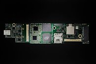
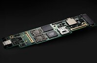
Today, Intel launched Intel Core processors with Intel Hybrid Technology, code-named "Lakefield." Leveraging Intel's Foveros 3D packaging technology and featuring a hybrid CPU architecture for power and performance scalability, Lakefield processors are the smallest to deliver Intel Core performance and full Windows compatibility across productivity and content creation experiences for ultra-light and innovative form factors.

"Intel Core processors with Intel Hybrid Technology are the touchstone of Intel's vision for advancing the PC industry by taking an experience-based approach to designing silicon with a unique combination of architectures and IPs. Combined with Intel's deepened co-engineering with our partners, these processors unlock the potential for innovative device categories of the future," said Chris Walker, Intel corporate vice president and general manager of Mobile Client Platforms.

Intel "Elkhart Lake" Processor Put Through 3DMark

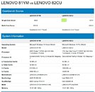
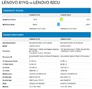
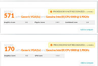
One of the first performance benchmarks of Intel's upcoming low-power processor codenamed "Elkhart Lake," surfaced on the Futuremark database, courtesy of TUM_APISAK. The chip scores 571 points, with a graphics score of 590 and physics score of 3801. The graphics score of the Gen11-based iGPU is behind the Intel UHD 630 gen 9.5 iGPU found in heavier desktop processors since "Kaby Lake," but we predict it's being dragged behind by the CPU (3801 points physics vs. roughly 17000 points of a 6-core "Coffee Lake" processor. The chip goes on to score 170 points in Time Spy, with 148 points graphics- and 1131 points physics-scores. Perhaps Cloud Gate would've been a more apt test.

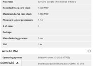
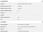
The "Elkhart Lake" silicon is built on Intel's 10 nm silicon fabrication process, and will power the next generation of Pentium Silver and Celeron processors. The chip features up to 4 CPU cores based on the "Tremont" low-power architecture, and an iGPU based on the newer Gen11 architecture. It features a single-channel memory controller that supports DDR4 and LPDDR4/x memory types. The chip in these 3DMark tests is a 4-core variant, likely a Pentium Silver engineering sample, with its CPU clocked at 1.90 GHz, and is paired with LPDDR4x memory. The chip comes in 5 W, 9 W, and 12 W TDP variants.

Intel Reassures Investors of its Server Processor Roadmap: Ice Lake-SP in 2020, Sapphire Rapids in 2021

Intel's Investor Relations head Trey Campbell, in a "fire-side chat" with top investors at the Cowen Virtual Technology Media and Telecom Conference, reaffirmed Intel's commitment to its server processor roadmap. Intel is on course to introducing its 10 nm Xeon "Ice Lake-SP" enterprise processor family by the end of 2020, and "Sapphire Rapids" sometime within 2021.

"Ice Lake-SP" processor will introduce the new "Whitley" platform, with a new 4,189-pin LGA socket, which leverages PCI-Express gen 4.0. While retaining the DDR4 memory standard, the memory interface has been broadened to 8-channel, and reference memory clock speeds are expected to be increased to DDR4-3200. The company's "Sapphire Rapids" processor is expected to shake up the market, as it introduces next-generation I/O, when it launches alongside the "Eagle Stream" platform in 2021. The processor will be built on the refined 10 nm+ silicon fabrication node, feature "Willow Cove" CPU cores, and I/O feature set that sees the introduction of DDR5 memory standard, and PCI-Express gen 5.0.

Intel "Elkhart Lake" Atom Processor Surfaces on Chinese Components Marketplace, "Tremont" Meets Gen11

Intel's next-generation Atom processor is codenamed "Elkhart Lake." Built on the 10 nm silicon fabrication process, the chip combines up to four CPU cores based on the "Tremont" microarchitecture, with an iGPU based on the Gen11 architecture, and a single-channel memory interface that supports DDR4 and LPDDR4. Differentiation of the processor include 2-core and 4-core CPU variants, and TDP variants spanning 6 W, 9 W, and 12 W. "Tremont" is a lightweight CPU core by Intel that lacks AVX capabilities. Besides "Elkhart Lake," the core is featured in the "Lakefield" Core heterogenous processors as the their low-power cores.

Chinese electronics B2B marketplace CogoBuy.com has the processor listed, although without listing out any processor model numbers. The marketplace is accepting RFQs (requests for quotations) for bulk purchase of these BGA chips on trays, without listing prices. Also listed is an "industrial variant" of the chip, which has an increased TJmax of 110 °C (compared to 105 °C of the standard variant). The Gen11 iGPU wasn't detailed, but it's likely to have a lower execution unit count than the variant found on "Ice Lake" processors, while retaining its display- and media-engines (ability to pull 8K60 displays).

Intel Rocket Lake CPU Appears with 6 Cores and 12 Threads

We have been hearing a lot about Intel's Rocket Lake lineup of processors. They are supposed to be a backport of Willow Cove 10 nm core, adapted to work on a 14 nm process for better yielding. Meant to launch sometime around late 2020 or the beginning of 2021, Rocket Lake is designed to work on the now existing LGA1200 socket motherboards, which were launched just a few days ago along with Intel Comet Lake CPUs. Rocket Lake is there to supply the desktop segment and satisfy user demand, in light of lacking 10 nm offers for desktop users. The 10 nm node is going to present only on mobile/laptop and server solutions before it comes to the desktop.

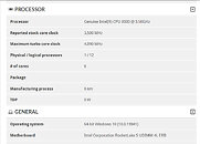
In the latest report on 3D Mark, the hardware leaker TUM APISAK has found a Rocket Lake CPU running the benchmark and we get to see first specifications of the Rocket Lake-S platform. The benchmark ran on 6 core model with 12 threads, that had a base clock of 3,5 GHz. The CPU managed to boost up to 4,09 GHz, however, we are sure that these are not final clocks and the actual product should have even higher frequencies. Paired with Gen12 Xe graphics, the Rocket Lake platform could offer a very nice alternative to AMD offerings if the backport of Willow Cove goes well. Even though it is still using a 14 nm node, performance would be good. The only things that would be sacrificed (from backporting) are die space and efficiency/heat.
Intel Rocket Lake Benchmark Report

Intel Tiger Lake Processor Spotted with Boost of 5 GHz

Intel is preparing to launch its next-generation Tiger Lake lineup of processors for the middle of 2020. The processors are based on the new "Willow Cove" CPU core, which supposedly brings even more IPC gains compared to previous "Golden Cove" CPU cores found in Ice Lake processors. The Tiger Lake lineup will use Intel's advanced 10 nm+ manufacturing process. This alone should bring some gains in frequency compared to the 10 nm Ice Lake processor generation, which was spotting a maximum of 4.1 GHz boost frequency on 28 W TDP model named Core i7-1068NG7. This processor is labeled as the highest-performing Ice Lake parts available today and the best 10 nm products available so far from Intel.

Thanks to the popular hardware leaker Rogame, we have evidence that the gains from 10 nm+ manufacturing process are real and that Tiger Lake will show us an amazing boost frequency of 5 GHz. In the benchmark, an unknown OEM laptop was spotted running the benchmark with a Tiger Lake CPU. This CPU is a 4 core, 8 threaded model with a base frequency of 2.3 GHz and a surprising boost frequency of 5 GHz. This information should, of course, be taken with a grain of salt until we get more information about the Tiger Lake lineup and their specifications.
Intel Tiger Lake Benchmark Report

Intel Updates x86/x64 Software Developer Manual With Tremont Architecture Details

Intel has today released the 43rd edition of its x86/x64 ISA developer manual designed to help developers see what's new in x86 world and make software optimizations for Intel's platform. In the latest edition of the manual, Intel has revealed the details of its low-power x86 "Tremont" architecture designed for 10 nm efficient, low-power computing. Announced last year in October, Intel promised to deliver a big IPC increase compared to the previous generation low-power CPU microarchitecture like the Goldmont Plus family. To achieve extra performance, Intel has implemented a lot of new solutions.

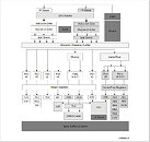
For starters, Tremont boasts better branch prediction unit, with increased capacity for instruction queue and better path-based conditional and indirect prediction. The front-end fetch and decode pipeline have been updated as well. Now the design is a 6-wide Out of Order Execution (OoOE) pipeline which can process 6 instructions per cycle. The Data cache is now upgraded to 32 KB. The load and store execution pipelines are now doubled and they are capable of two loads and two stores, or one load and one store, depending on the application. Tremont also updates on one important point and that is a dedicated store data port for integer and vector integer/floating-point data. Another big improvement is happening in the cryptography department. Tremont now features Galois-field instructions labeled as the GFNI family of instructions. There are two AES units for faster AES encryption and decryption. The already implemented SHA-NI cryptography standard was enhanced and it now is much faster as well. For mode in-depth report please check out Intel's x86/x64 manual.
Intel Tremont

GDP WIN Max Handheld Game Console Obliterates Indiegogo Funding Goal

The GDP WIN Max is the latest handheld PC from GDP, described as an all in one product that combines the portability of a handheld and the graphics performance of a gaming laptop. The GDP WIN Max has smashed its Indiegogo funding goal of $25,000 currently sitting at over $1,300,000 USD, the handled PC features vastly upgraded internal from the GDP WIN 2 now featuring a 10th generation 10 nm Intel Core I5-1035G7 CPU with Iris Plus Graphics 940, paired with 16 GB of DDR4 3733 MHz ram, 512 GB M.2 SSD and 8" HD screen. The GDP WIN Max is on sale at a special crowdfunding price of $779 USD.

Intel Jasper Lake CPU Appears with Gen11 Graphics

Intel is preparing to update its low-end segment designed for embedded solutions, with a next-generation CPU codenamed Jasper Lake. Thanks to the popular hardware finder and leaker, _rogame has found a benchmark showing that Intel is about to bless low-end with a lot of neat stuff. The benchmark results show a four-core, four threaded CPU running at 1.1 GHz base clock with a 1.12 GHz boost clock. Even though these clocks are low, this is only a sample and the actual frequency will be much higher, expecting to be near 3 GHz. The CPU was spotted in a configuration rocking 32 GB of DDR4 SODIMM memory.

Jasper Lake is meant to be a successor to Gemini Lake and it will use Intel's Tremont CPU architecture designed for low-power scenarios. Designed on a 10 nm manufacturing node from Intel, this CPU should bring x86 processors to a wide range of embedded systems. Although the benchmark didn't mention which graphics the CPU will be paired with, _rogame speculates that Intel will use Gen11 graphics IP. That will bring a nice update over Gemini Lake's Gen9.5 graphics. That alone should bring better display output options and more speed. These CPUs are designed for Atom/Pentium/Celeron lineup, just like Gemini Lake before them.

Update: Updated the article to reflect the targeted CPU category.
Intel Tremont Intel Jasper Lake

SMIC Begins Mass-Production of 14nm FinFET SoCs for Huawei HiSilicon

Semiconductor Manufacturing International Corporation (SMIC), the state-backed Mainland Chinese semiconductor foundry, announced that it commenced mass-production of 14 nm FinFET SoCs for Huawei's HiSilicon subsidiary, a mere one month since Huawei shifting chip orders from TSMC to it. The company is manufacturing Kirin 710A is a revision of the original Kirin 710 SoC from 2018, built on SMIC's 14 nm node. The 4G-era SoC is capable of powering mid-range smartphones for Huawei's Honor brand, and uses an Arm big.LITTLE setup of Cortex A53 and Cortex A57 cores. This represents a major milestone not just for SMIC, but also Huawei, which has seen the company's isolation from cutting-edge overseas fabs such as TSMC. Much of Huawei's fate is riding on the success of SMIC's next-generation N+1 node, which purportedly offers a 57 percent energy-efficiency gain over 14 nm FinFET, rivaling sub-10 nm nodes such as 7 nm; enabling Huawei to build 5G-era SoCs.

Intel Xe DG1 Silicon Not Meant for Desktop Add-on Cards, Only as an MGPU

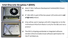
Intel's 10 nm Xe DG1 silicon made its first public appearance as the DG1-SDV (software development vehicle), a desktop PCIe graphics cards that Intel shipped out to its ISVs (independent software vendors), allowing them to begin preparing software for the Xe architecture. Argonne National Laboratory, the organization behind the Aurora Supercomputing Project that implements Xe HP "Ponte Vecchio" super-scalar compute processors, in its presentation, took a brief technical detour talking a bit about the DG1-SDV.

In the presentation, it is revealed that Intel will indeed monetize (or "productize") the silicon at the heart of the DG1-SDV, only not as a desktop graphics card. The chip will be sold as a mobile GPU, not even as an MXM, but as a GPU meant to be hardwired along with its dedicated memory onto notebooks' mainboards. We predict Intel is attempting to tap into the market segment where NVIDIA sells its GeForce MX300 line of entry-level discrete GPUs. Earlier this week, we spotted a discrete GPU with the specs of the DG1 having significantly increased 1.50 GHz GPU clocks, resulting in a FP32 throughput rivaling the AMD Radeon RX 560 or the "Vega" based iGPU of "Renoir." The Xe architecture will also be released as an iGPU solution, powering Intel's "Tiger Lake" Core mobile processor. Find the Aurora presentation here (PDF).

Intel Reports First-Quarter 2020 Financial Results

Intel Corporation today reported first-quarter 2020 financial results. "Our first-quarter performance is a testament to our team's focus on safeguarding employees, supporting our supply chain partners and delivering for our customers during this unprecedented challenge," said Bob Swan, Intel CEO."The role technology plays in the world is more essential now than it has ever been, and our opportunity to enrich lives and enable our customers' success has never been more vital. Guided by our cultural values, competitive advantages and financial strength, I am confident we will emerge from this situation an even stronger company."

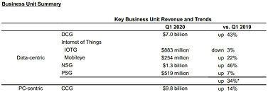
In the first quarter, Intel achieved 34 percent data-centric revenue growth and 14 percent PC-centric revenue growth YoY. The company maintained essential factory operations with greater than 90 percent on-time delivery while supporting employees, customers and communities in response to the COVID-19 pandemic. This includes a new Intel Pandemic Response Technology Initiative to combat the virus where we can uniquely make a difference with Intel technology, expertise, and resources.

Intel's Next-Generation Tiger Lake-U Core i7-1165G7 CPU Score Leaks

Intel is preparing to launch its next-generation Tiger Lake-U lineup of CPUs based on the new Willow Cove core that is supposed to bring big IPC gains and plenty of new features. Being a part of the 11th generation of Core CPUs, these processors are expected to arrive sometime in the second half of 2020, built on Intel's 10 nm+ manufacturing process. Thanks to a popular hardware leaker @_rogame, we have found another Tiger Lake-U in the 3D Mark benchmark database. Unlike the last time when we saw Intel's Core i7-1185G7 being run on the 3D Mark tests, we now have test results of its brother - the Core i7-1165G7.

From the 3D Mark report, we can see some details like CPU's base frequency, which is 2.8 GHz in this case. This is just 200 MHz lower compared to the previous Core i7-1185G7 CPU that leaked. The platform used to test the new Core i7-1165G7 CPU was running Windows 10 and had 16 GB of DDR4 SODIMM memory. The new 3D Mark results are already looking promising. From the previous leak of Core i7-1185G7, we saw that Tiger Lake CPU which managed to score 2922 in the CPU test, 1296 in GPU test, and an overall score of 1414. However, this new Core i7-1165G7 CPU is a bit different. In the graphic test, it scores 1150 points, while the CPU test shows an impressive 4750 points. This Core i7-1165G7 result is much higher compared to the more powerful Core i7-1185G7 CPU, which is a bit strange. It could be attributed to a faster memory, but so far we don't know. However, the overall score of the i7-1165G7 is a bit lower compared to i7 1185G7, scoring 1297 points.
Intel Core i7-1165G7

Intel 10nm Product Lineup for 2020 Revealed: Alder Lake and Ice Lake Xeons

A leaked Intel internal slide surfaced on Chinese social networks, revealing five new products the company will build on its 10 nm silicon fabrication process. These include the "Alder Lake" heterogenous desktop processor, "Tiger Lake" mobile processor, "Ice Lake" based Xeon Scalable enterprise processors, DG1 discrete GPU, and "Snow Ridge" 5G base-station SoC. Some, if not all of these products, will implement Intel's new 10 nm+ silicon fabrication node that is expected to go live within 2020.

"Alder Lake" is a desktop processor that implements Intel's new heterogenous x86 core design that's making its debut with "Lakefield." The chip features up to 8 larger "Willow Cove" or "Golden Cove" CPU cores, and up to 8 smaller "Tremont" or "Gracemont" cores. This 8-big/8-small combo lets the chip achieve TDP targets around 80 Watts. Next up is "Tiger Lake," Intel's next-generation mobile processor family succeeding "Ice Lake." This microarchitecture implements "Willow Cove" CPU cores in a homogeneous setup, alongside Xe architecture based integrated graphics. "Ice Lake-SP" is Intel's next enterprise architecture that places mature "Sunny Cove" CPU cores in extreme core-count dies. Lastly, there's "Snow Ridge," an SoC purpose built for 5G base-stations. Image quality notwithstanding, these slides don't appear particularly new, and it's likely that COVID-19 has destabilized the roadmap. For instance, "Alder Lake," and "Ice Lake-SP" are expected to be 10 nm++ chips, a node that doesn't go live before 2021.

Samsung Announces Industry's First EUV DRAM with Shipment of First Million Modules

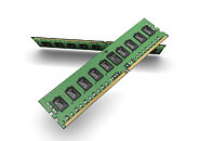
Samsung Electronics Co., Ltd., the world leader in advanced memory technology, today announced that it has successfully shipped one million of the industry's first 10 nm-class (D1x) DDR4 (Double Date Rate 4) DRAM modules based on extreme ultraviolet (EUV) technology. The new EUV-based DRAM modules have completed global customer evaluations, and will open the door to more cutting-edge EUV process nodes for use in premium PC, mobile, enterprise server and datacenter applications.

"With the production of our new EUV-based DRAM, we are demonstrating our full commitment toward providing revolutionary DRAM solutions in support of our global IT customers," said Jung-bae Lee, executive vice president of DRAM Product & Technology at Samsung Electronics. "This major advancement underscores how we will continue contributing to global IT innovation through timely development of leading-edge process technologies and next-generation memory products for the premium memory market."
Samsung EUV DDR4

Intel Core i5-L15G7 Lakefield Processor Spotted

Intel has been experimenting with a concept of mixing various types of cores in a single package with a design called Lakefield. With this processor, you would get a package of relatively small dimensions that are 12-by-12-by-1 millimeters withing very low TDP. Thanks to the Twitter user InstLatX64 (@InstLatX64) we have some GeekBench 5 results of the new Lakefield chip. The CPU in question is the Core i5-L15G7, a 5 core CPU without HyperThreading. The 5C/5T would be a weird configuration if only Lakefield wasn't meant for such configs. There are one "big" Sunny Cove core and four "small" Tremont cores built on the 10 nm manufacturing process. This is the so-called compute die, where only the CPU cores are present. The base dies containing other stuff like I/O controllers and PHYs, memory etc. is made on a low-cost node like 22 nm, where performance isn't the primary target. The whole chip is targeting the 5-7 W TDP range.

In the GeekBench 5 result we got, the Core i5-L15G7 is a processor that has a base frequency of 1.4 GHz, while in the test it reached as high as 2.95 GHz speeds. This is presumably for the big Sunny Cove cores, as Tremont cores are supposed to be slower. The cache configuration reportedly puts 1.5 MB of L2$ and 4 MB of L3$ for the CPUs. If we take a look at performance numbers, the chip scores 725 points in single-core tests, while the multi-core result is 1566 points. We don't know what is the targeted market and what it competes with, however, if compared to some offerings from Snapdragon, like the Snapdragon 835, it offers double the single-threaded performance with a similar multi-core score. If this is meant to compete with the more powerful Snapdragon offerings like the 8cx model, comparing the two results in Intel's fail. While the two have similar single-core performance, the Snapdragon 8cx leads by as much as 76.9% in a multi-core scenario, giving this chip a heavy blow.
Intel Core i5-L15G7 Intel Lakefield

Intel Courts TSMC 6nm and 3nm Nodes for Future Xe GPU Generations

Intel is rumored to be aligning its future-generation Xe GPU development with TSMC's node development cycle, with the company reportedly negotiating with the Taiwanese foundry for 6 nm and 3 nm allocation for its large Xe GPUs. Intel's first Xe discrete GPUs for the market, however, are reportedly built on the company's own 10 nm+ silicon fabrication process.

While Intel's fascination with TSMC 3 nm is understandable, seeking out TSMC's 6 nm node raises eyebrows. Internally referred to as "N6," the 6 nm silicon fabrication node at TSMC is expected to go live either towards the end of 2020 or early 2021, which is when Intel's 10 nm+ node is expected to pick up volume production, beginning with the company's "Tiger Lake" processors. Perhaps a decision has been made internally to ensure that Xe doesn't eat too much into Intel's own foundry capacities meant for processor manufacturing, and to instead outsource Xe manufacturing to third-party foundries like TSMC and Samsung eventually. Way back in April 2019 it was rumored that Intel was evaluating Samsung as a foundry partner for Xe.

Rumor: Intel to Introduce Big.Little Architecture for Desktop With Alder Lake-S, New LGA 1700 Socket

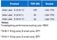
Hold on to your helmets: a wild rumor that Intel may be looking to introduce the same design considerations as they already did with their Lakefield architecture has appeared. According to momomo via Twitter (a user who has already shared many rumors and details in the PC hardware space) as well as some other sources, Intel is looking to bring a Big.Little-like design (which Intel calls Hybrid architecture) to the desktop platform in the form of Alder Lake-S, to be reportedly built on the 10 nm process. While Intel's Lakefield (especially geared for the mobile market) only sported four Atom (Intel's low power) Tremont cores combined with one high-performance Sunny Cove core, Alder Lake-S could sport as many as an 8+8 configuration, with a TDP currently set up to 80 W (and up to 125 W TDP is also set in the revealing slides with a disclosure regarding investigating performance scaling in up to 150 W TDP).

Should this actual Alder Lake-S product materialize in the 10 nm process, this could be a way for Intel to salvage what it can from the 10 nm process for the desktop platform. As we know from multiple reports on the state of Intel's 10 nm, yields and operating frequencies aren't close to what was expected, and Intel's CFO George Davis even said at last week's Morgan Stanley's Analyst Conference that their 10 nm process wouldn't be as profitable as even 22 nm, which does show that Intel is already looking past this process for their 7 nm deployment. A Big.Little design for a desktop architecture does seem like a more plausible design decision for a struggling process than a full 16-core monolithic die such as those Intel currently employs.
Intel Alder Lake S Lineup Intel CPU Roadmap

Samsung Begins Mass Production of Industry's First 16GB LPDDR5 DRAM

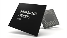
Samsung Electronics, a world leader in advanced memory technology, today announced that it has begun mass producing the industry's first 16-gigabyte (GB) LPDDR5 mobile DRAM package for next-generation premium smartphones. Following mass production of the industry-first 12 GB LPDDR5 in July, 2019, the new 16 GB advancement will lead the premium mobile memory market with added capacity that enables enhanced 5G and AI features including graphic-rich gaming and smart photography.

"Samsung has been committed to bringing memory technologies to the cutting edge in allowing consumers to enjoy amazing experiences through their mobile devices. We are excited to stay true to that commitment with our new, top-of-the-line mobile solution for global device manufacturers," said Cheol Choi, senior vice president of memory sales & marketing, Samsung Electronics. "With the introduction of a new product lineup based on our next-generation process technology later this year, Samsung will be able to fully address future memory demands from global customers."

Intel Zooms in on "Lakefield" Foveros Package

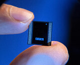
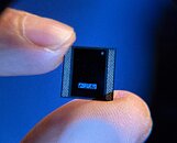
The fingernail-size Intel chip with Foveros technology is a first-of-its kind. With Foveros, processors are built in a totally new way: not with the various IPs spread out flat in two dimensions, but with them stacked in three dimensions. Think of a chip designed as a layer cake (a 1-millimeter-thick layer cake) versus a chip with a more-traditional pancake-like design. Intel's Foveros advanced packaging technology allows Intel to "mix and match" technology IP blocks with various memory and I/O elements - all in a small physical package for significantly reduced board size. The first product designed this way is "Lakefield," the Intel Core processor with Intel hybrid technology.

Industry analyst firm The Linley Group recently named Intel's Foveros 3D-stacking technology as "Best Technology" in its 2019 Analysts' Choice Awards. "Our awards program not only recognizes excellence in chip design and innovation, but also acknowledges the products that our analysts believe will have an impact on future designs," said Linley Gwennap, of The Linley Group.

Samsung Launches 3rd-Generation "Flashbolt" HBM2E Memory

Samsung Electronics, the world leader in advanced memory technology, today announced the market launch of 'Flashbolt', its third-generation High Bandwidth Memory 2E (HBM2E). The new 16-gigabyte (GB) HBM2E is uniquely suited to maximize high performance computing (HPC) systems and help system manufacturers to advance their supercomputers, AI-driven data analytics and state-of-the-art graphics systems in a timely manner.

"With the introduction of the highest performing DRAM available today, we are taking a critical step to enhance our role as the leading innovator in the fast-growing premium memory market," said Cheol Choi, executive vice president of Memory Sales & Marketing at Samsung Electronics. "Samsung will continue to deliver on its commitment to bring truly differentiated solutions as we reinforce our edge in the global memory marketplace."

Intel Core i5-L16G7 is the first "Lakefield" SKU Appearance, Possible Prelude to New Nomenclature?

Intel Core i5-L16G7 is the first commercial SKU that implements Intel's "Lakefield" heterogenous x86 processor architecture. This 5-core chip features one high-performance "Sunny Cove" CPU core, and four smaller "Tremont" low-power cores, with an intelligent scheduler balancing workloads between the two core types. This is essentially similar to ARM big.LITTLE. The idea being that the device idles most of the time, when lower-powered CPU cores can hold the fort; performance cores kick in only when really needed, until which time they remain power-gated. Thai PC enthusiast TUM_APISAK discovered the first public appearance of the i5-L16G7 in an unreleased Samsung device that has the Userbenchmark device ID string "SAMSUNG_NP_767XCL."

Clock speeds of the processor are listed as "1.40 GHz base, with 1.75 GHz turbo," but it's possible that the two core types have different clock-speed bands, just like the cores on big.LITTLE SoCs. Other key components of "Lakefield" include an iGPU based on the Gen11 graphics architecture, and an LPDDR4X memory controller. "Lakefield" implements Foveros packaging, in which high-density component dies based on newer silicon fabrication nodes are integrated with silicon interposers based on older fabrication processes, which facilitate microscopic high-density wiring between the dies. In case of "Lakefield," the Foveros package features a 10 nm "compute field" die sitting atop a 22 nm "base field" interposer.
Return to Keyword Browsing
Dec 18th, 2024 01:35 EST change timezone

New Forum Posts

Popular Reviews

Controversial News Posts