News Posts matching #10 nm

Return to Keyword Browsing

Intel Says Its Upcoming Gen12 GPUs Will Feature Biggest Architecture Change In A Decade

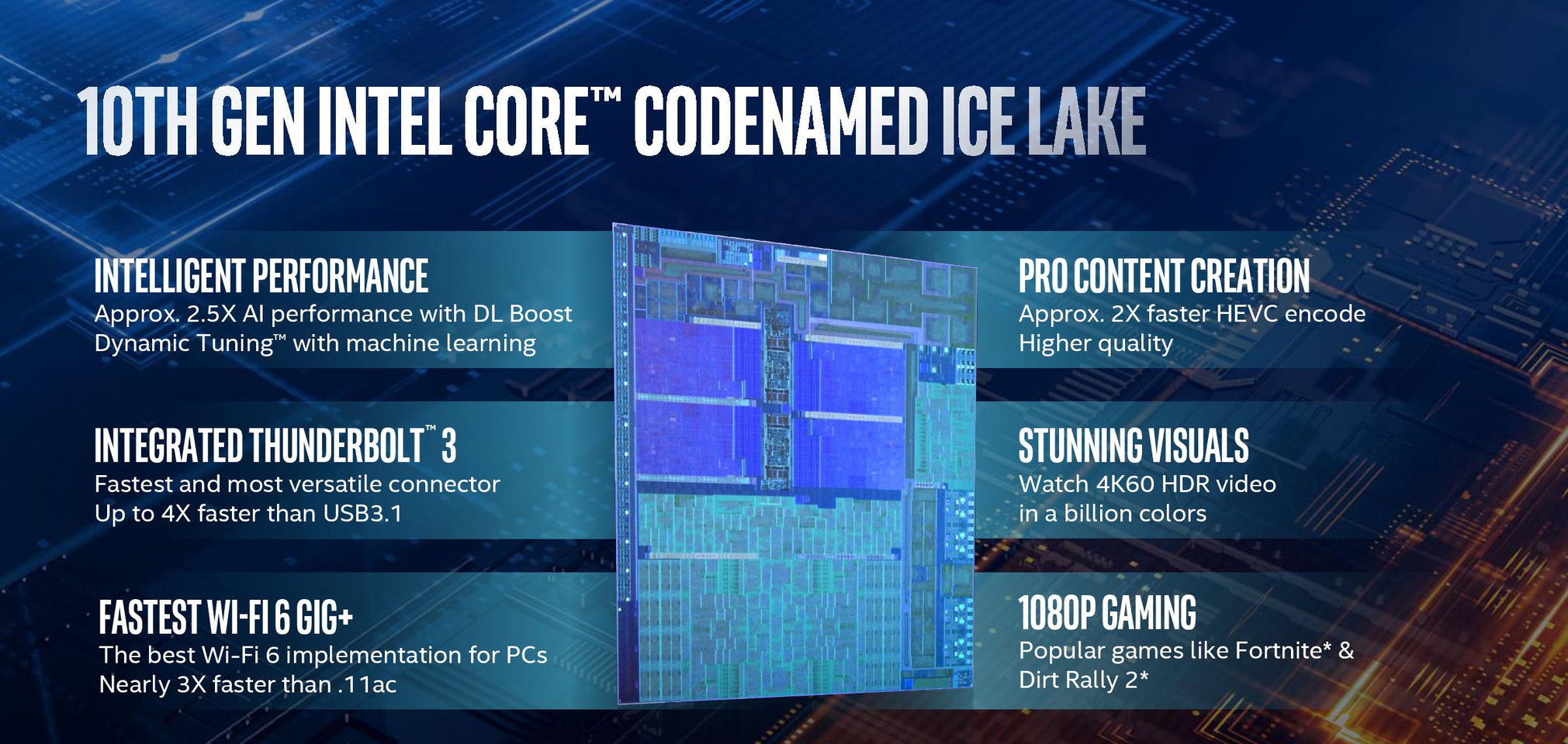
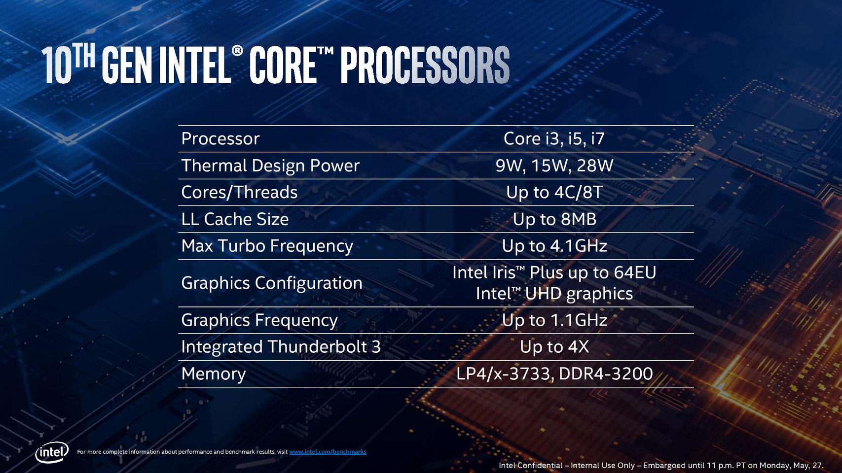
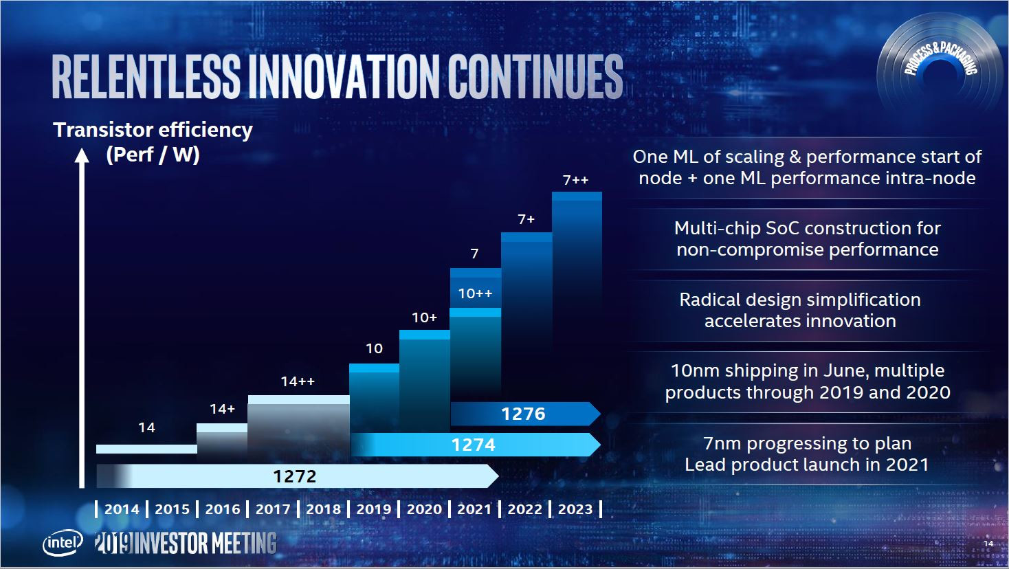
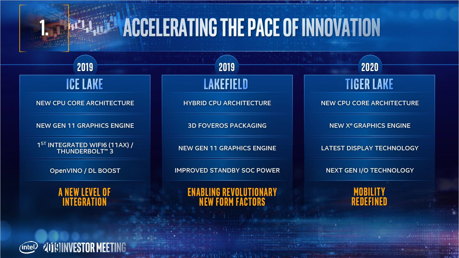
Intel is slowly realizing plans to "one up" its GPU game starting from first 10 nm Ice Lake CPUs that feature Gen11 graphics, equipping users of integrated GPUs with much more performance than they previously got. Fortunately, Intel doesn't plan to stop there. Thanks to the recent pull request found on GitLab Mesa repository, we can now expect to receive biggest GPU performance bump in over a decade with the arrival of Gen12 based GPUs, found on next generation Tiger Lake processors.

In this merge request, Francisco Jerez, member of Intel's open source Linux graphics team, stated the following: "Gen12 is planned to include one of the most in-depth reworks of the Intel EU ISA since the original i965. The encoding of almost every instruction field, hardware opcode and register type needs to be updated in this merge request. But probably the most invasive change is the removal of the register scoreboard logic from the hardware, which means that the EU will no longer guarantee data coherency between register reads and writes, and will require the compiler to synchronize dependent instructions anytime there is a potential data hazard..."

LGA 4189 is the Latest Socket for Intel's Next Generation of Xeon CPUs

TE Connectivity, the maker of various kinds of connectivity solutions for computer systems, has released its latest iteration of the LGA socket for the next generation of Xeon Scalable CPUs. Being validated by Intel, the LGA 4189-4 and LGA 4189-5 are going to power the next generation of 10 nm Xeon CPUs, based on the Ice Lake architecture, and up to 56-core 2nd generation Xeon Scalable CPUs. While there are two models of the socket, TE Connectivity didn't reveal what the differences are between them. Socket P4 (LGA 4189-4) and P5 (LGA 4189-5) also feature exactly the same pin count, 0.9906 mm hex pitch and 2.7 mm SP height, so we can only speculate that the "4" or "5" in the revision is supposed to indicate details like higher power delivery capability or support for Ice Lake CPUs.

In addition to providing a new socket for Ice Lake, these sockets have support for PCI-Express Gen 4.0 and eight-channel memory (supported memory configurations are vendor dependent), meaning that we are getting two more memory channels than previous Xeon CPUs with a faster and newer PCIe standard.

Intel Ships First 10nm Agilex FPGAs

Intel today announced that it has begun shipments of the first Intel Agilex field programmable gate arrays (FPGAs) to early access program customers. Participants in the early access program include Colorado Engineering Inc., Mantaro Networks, Microsoft and Silicom. These customers are using Agilex FPGAs to develop advanced solutions for networking, 5G and accelerated data analytics.

"The Intel Agilex FPGA product family leverages the breadth of Intel innovation and technology leadership, including architecture, packaging, process technology, developer tools and a fast path to power reduction with eASIC technology. These unmatched assets enable new levels of heterogeneous computing, system integration and processor connectivity and will be the first 10nm FPGA to provide cache-coherent and low latency connectivity to Intel Xeon processors with the upcoming Compute Express Link," said Dan McNamara, Intel senior vice president and general manager of the Networking and Custom Logic Group.

AMD Designing Zen 4 for 2021, Zen 3 Completes Design Phase, out in 2020

AMD in its 2nd generation EPYC processor launch event announced that it has completed the design phase of its next-generation "Zen 3" CPU microarchitecture, and is currently working on its successor, the "Zen 4." AMD debuted its "Zen 2" microarchitecture with the client-segment 3rd generation Ryzen desktop processor family, it made its enterprise debut with the 2nd generation EPYC. This is the first x86 CPU microarchitecture designed for the 7 nanometer silicon fabrication process, and is being built on a 7 nm DUV (deep ultraviolet) node at TSMC. It brings about double-digit percentage IPC improvements over "Zen+."

The "Zen 3" microarchitecture is designed for the next big process technology change within 7 nm, EUV (extreme ultraviolet), which allows significant increases in transistor densities, and could facilitate big improvements in energy-efficiency that could be leveraged to increase clock-speeds and performance. It could also feature new ISA instruction-sets. With "Zen 3" passing design phase, AMD will work on prototyping and testing it. The first "Zen 3" products could debut in 2020. "Zen 4" is being designed for a different era.

Intel Starts Shipping 10 nm Ice Lake CPUs to OEMs

During its second quarter earnings call, Intel announced that it has started shipping of 10th generation "Core" CPUs to OEMs. Making use of 10 nm lithography, the 10th generation of "Core" CPUs, codenamed Ice Lake, were qualified by OEMs earlier in 2019 in order to be integrated into future products. Ice Lake is on track for holiday season 2019, meaning that we can expect products on-shelves by the end of this year. That is exciting news as the 10th generation of Core CPUs is bringing some exciting micro-architectural improvements along with the long awaited and delayed Intel's 10nm manufacturing process node.

The new CPUs are supposed to get around 18% IPC improvement on average when looking at direct comparison to previous generation of Intel CPUs, while being clocked at same frequency. This time, even regular mobile/desktop parts will get AVX512 support, alongside VNNI and Cryptography ISA extensions that are supposed to bring additional security and performance for the ever increasing number of tasks, especially new ones like Neural Network processing. Core configurations will be ranging from dual core i3 to quad core i7, where we will see total of 11 models available.

Intel "Tremont" Low-power CPU to Feature L3 Cache

Intel's next-generation Pentium Silver "Snow Ridge" SoC, featuring "Tremont" CPU cores, could see the debut of an L3 cache to the segment. Intel CPU cores in this segment, such as the "Goldmont Plus," only feature shared L2 caches across 4-core modules. The introduction of L3 cache was indicated by a new performance counter "MEM_LOAD_UOPS_RETIRED_L3_HIT," with a description clearly mentioning a "level 3 cache." The introduction of L3 cache as the SoC's LLC (last level cache) could mean Intel is trying to improve inter-component communication by introducting the L3 cache as "town-square" for the various components of the SoC, such as the CPU cores, the iGPU, and the integrated chipset. The company could deploy a ring-bus interconnect that has ring-stops at the various components, and slices of this L3 cache. Intel is building the "Snow Ridge" silicon on its swanky new 10 nm silicon fabrication process, and the chip could see a 2020 debut targeting network infrastructure devices.

Intel Puts Out More Official-looking Renders of the Xe Graphics Card

Intel China through its Weibo (Twitter-equivalent) handle put out more official-looking renders of its Xe graphics card. The Weibo post doesn't cite an author, leading us to speculate that the company's industrial design team is close to finalizing a product-design for at least the client-segment derivative of Xe. The swanky-looking card apparently has a stamped metal cooler shroud, a cooling solution that's based on a fin-stack heatsink that's ventilated by three fans, and quite some LED embellishment. An interesting design detail is the exponent symbol projected on the center fan. The power inputs are located at the tail end of the card, which is where most professional graphics cards have them; and consist of a pair of 8-pin PCIe inputs. Display inputs include three DisplayPorts, and an HDMI. The first Xe graphics card bound for 2020 will be built on Intel's 10 nm silicon fabrication process, which offers comparable transistor-densities to current 7 nm nodes.

ADATA Shows Off a JEDEC-compliant 32GB Dual-rank DIMM That Isn't "Double Capacity"

Last year, with the introduction of the Intel Z390 chipset, there was a spate of so-called "double capacity DIMMs" or DC DIMMs, tall memory modules with two rows of DRAM chips, which added up to 32 GB per DIMM. You needed a Z390 platform and a 9th generation Core processor that supported up to 128 GB of memory, to use these things. With the introduction of 16 Gb DDR4 DRAM chips by both Micron and Samsung, JEDEC-compliant 32 GB unbuffered DIMMs of standard height are finally possible, and ADATA put together the first of these, shown off at Computex 2019.

The AD4U2666732GX16 is a 32-gigabyte dual-rank unbuffered DIMM made using 16 Gb chips supplied by Micron Technology. The modules tick at JEDEC-standard DDR4-2666 speeds, at a module voltage of 1.2 Volts. ADATA didn't disclose timings. The 16 Gb DRAM chips are made by Micron in an advanced (3rd generation) 10 nm-class silicon fabrication process to achieve the desired transistor-density. 32 GB DIMMs are expected to hit critical-mass in 2H-2019/2020, with the advent of AMD's 3rd generation Ryzen "Matisse," and Intel's "Ice Lake-S" desktop processors. Memory manufacturers are also expected to put out speedy and highly-compatible single-rank 16-gigabyte DIMMs using 16 Gb chips, which could finally make 32 GB dual-channel the mainstream memory configuration, moving up from half a decade of 2x 8 GB.

Intel 10th Generation Core Case-badges Revealed

Intel laid rest to speculation that post 9th generation, it could replace its Core brand with something else. The 10th generation Core processors, built around the 10 nm "Ice Lake" microachitecture, will feature the first noteworthy IPC increments since "Skylake" thanks to their new "Sunny Cove" CPU cores. These will also feature DLBoost, a fixed-function matrix-multiplication hardware that speeds up deep-neural net building and training by 5x, as well as certain AVX-512 instructions. The cores will be optimized to cope with 2.4 Gbps 802.11ax Wi-Fi and faster Ethernet standards. The first of these chips will target mobile computing platforms, and will be quad-core parts like the dies pictured below. To save notebook PCB real-estate, Intel will put the processor and PCH dies into a multi-chip module. It will be quite a wait for the desktop implementation, but at least you know what their case-badges look like.

Intel Switches to a "Data Center First" Strategy with 7nm

Intel traditionally released new CPU microarchitectures and new silicon fabrication nodes with the client segment, and upon observing some degree of maturity with both, graduated them to the enterprise segment. With its homebrew 7 nanometer silicon fabrication process that takes flight in 2021, Intel will flip its roadmap execution strategy, by going "Data Center First." Speaking at the 2019 Investors Day summit, Intel SVP and GM of Data Center Group Navin Shenoy revealed that the first product built on Intel's 7 nm process will be a GPGPU accelerator chip derived from the Xe architecture for the Data Center, followed closely by a new server CPU. Both these products come under Shenoy's group. One is a competitor to likes of NVIDIA Tesla and AMD Radeon Instinct, while the other is a Xeon processor competing with AMD EPYC.

Shenoy explained the reason why within his group, the GPGPU product was prioritized over the server CPU. It has to do with redundancy of the GPU silicon, or specifically, the higher potential to harvest partially defective dies than CPU. A GPU has a larger number of indivisible components that can be disabled if found non-functional at the time of quality assurance, and these harvested dies can be used to carve out variants of a main product. An example of this would be NVIDIA carving out the GeForce GTX 1070 (1,920 CUDA cores) from the GP104 silicon that physically has 2,560 CUDA cores. The first manufacturing runs of the GPGPU will give the foundry valuable insights into the way the node is behaving, so it could be refined and matured for the server CPU. With 10 nm, however, Intel is sticking to the client-first model, by rolling out the "Ice Lake" processor towards the end of 2019. Within the Client Computing group, Intel has flipped its roadmap execution such that mobile (notebook) CPUs take precedence over desktop ones.

Intel "Tiger Lake" Architecture Combines Willow Cove CPU Cores and Xe iGPU

Even as Intel banks on 10 nm "Ice Lake" to pull it out of the 14 nm dark ages, the company is designing a fascinating new monolithic processor SoC die that succeeds it. Codenamed "Tiger Lake," and slated to debut in 2020, this die packs "Willow Cove" CPU cores and an iGPU based on Intel's Xe architecture, not Gen11. "Willow Cove" CPU cores are more advanced than the "Sunny Cove" cores "Ice Lake" packs, featuring a redesigned on-die cache, additional security features, and transistor optimization yielded from the newer 10 nm+ silicon fabrication process.

Intel is already boasting of 1 TFLOP/s compute power of the Gen11 iGPU on "Ice Lake," so it's logical to predict that the Xe based iGPU will be significantly faster. It will also support the latest display standards. The "next-gen I/O" referenced by Intel could be faster NVMe, Thunderbolt, and USB standards that leverage the bandwidth doubling brought about by PCI-Express gen 4.0. Here's the catch: much like "Ice Lake," the new "Tiger Lake" chip will get a mobile debut as Tiger Lake-Y or Tiger Lake-U, and desktop processors could follow later, possibly even 2021, depending on how much pressure it faces from AMD.

Intel Switches Gears to 7nm Post 10nm, First Node Live in 2021

Intel's semiconductor manufacturing business has had a terrible past 5 years as it struggled to execute its 10 nanometer roadmap forcing the company's processor designers to re-hash the "Skylake" microarchitecture for 5 generations of Core processors, including the upcoming "Comet Lake." Its truly next-generation microarchitecture, codenamed "Ice Lake," which features a new CPU core design called "Sunny Cove," comes out toward the end of 2019, with desktop rollouts expected 2020. It turns out that the 10 nm process it's designed for, will have a rather short reign at Intel's fabs. Speaking at an investor's summit on Wednesday, Intel put out its silicon fabrication roadmap that sees an accelerated roll-out of Intel's own 7 nm process.

When it goes live and fit for mass production some time in 2021, Intel's 7 nm process will be a staggering 3 years behind TSMC, which fired up its 7 nm node in 2018. AMD is already mass-producing CPUs and GPUs on this node. Unlike TSMC, Intel will implement EUV (extreme ultraviolet) lithography straightaway. TSMC began 7 nm with DUV (deep ultraviolet) in 2018, and its EUV node went live in March. Samsung's 7 nm EUV node went up last October. Intel's roadmap doesn't show a leap from its current 10 nm node to 7 nm EUV, though. Intel will refine the 10 nm node to squeeze out energy-efficiency, with a refreshed 10 nm+ node that goes live some time in 2020.

Intel to Use 5-digit Processor Model Numbering with 10th Gen?

A lot of us could be wondering how Intel could number its client-segment processors after the i9-9980XE, or the 9th generation Core in general, and hoping for a major branding change or at least a change in the model numbering scheme. It turns out, Intel will brazen it out with a 5-digit model number and stick to the current scheme. Going by this scheme, the successor to the Core i7-9700K could be the Core i7-10700K, for example. Intel jumped from 3-digit to 4-digit as it transitioned from 1st gen Core to 2nd gen as it ran out of 3-digit numbers with the Core i7-9xx. It's now running out of 4-digit numbers.

Evidence of 5-digit number surfaced when Thai enthusiast TUM_Apisak tweeted a screenshot of a UL Benchmarks Systeminfo page describing an unreleased Core i5-10210U, which is probably a mobile processor based on the 10 nm "Ice Lake-U" silicon slated for late-2019. With a nominal clock-speed of 1.60 GHz and "reported" speed of 2.10 GHz, the Turbo Boost frequency of this 4-core/8-thread chip is rated at almost 3.80 GHz. Japanese enthusiast Komachi Ensaka confirmed this with three other model numbers: i3-10110U, i5-10510U, and i7-10710U.

Intel 10nm Ice Lake to Quantitatively Debut Within 2019

Intel put out interesting details about its upcoming 10 nanometer "Ice Lake" CPU microarchitecture rollout in its recent quarterly financial results call. The company has started qualification of its 10 nm "Ice Lake" processors. This involves sending engineering samples to OEMs, system integrators and other relevant industry partners, and getting the chips approved for their future product designs. The first implementation of "Ice Lake" will not be a desktop processor, but rather a low-power mobile SoC designed for ultraportables, codenamed "Ice Lake-U." This SoC packs a 4-core/8-thread CPU based on the "Sunny Cove" core design, and Gen11 GT2 integrated graphics with 64 execution units and nearly 1 TFLOP/s compute power. This SoC will also support WiFi 6 and LPDDR4X memory.

Intel CEO Bob Swan also remarked that the company has doubled its 10 nm yield expectations. "On the [10 nm] process technology front, our teams executed well in Q1 and our velocity is increasing," he said, adding "We remain on track to have volume client systems on shelves for the holiday selling season. And over the past four months, the organization drove a nearly 2X improvement in the rate at which 10nm products move through our factories." Intel is prioritizing enterprise over desktop, as "Ice Lake-U" will be followed by "Ice Lake-SP" Xeon rollout in 2020. There was no mention of desktop implementations such as "Ice Lake-S." Intel is rumored to be preparing a stopgap microarchitecture for the desktop platform to compete with AMD "Matisse" Zen 2 AM4 processors, codenamed "Comet Lake." This is essentially a Skylake 10-core die fabbed on existing 14 nm++ node. AMD in its CES keynote announced an achievement of per-core performance parity with Intel, so it could be interesting to see how Intel hopes 10 "Skylake" cores match up to 12-16 "Zen 2" cores.

Intel Reports First-Quarter 2019 Financial Results

Intel Corporation today reported first-quarter 2019 financial results. "Results for the first quarter were slightly higher than our January expectations. We shipped a strong mix of high performance products and continued spending discipline while ramping 10nm and managing a challenging NAND pricing environment. Looking ahead, we're taking a more cautious view of the year, although we expect market conditions to improve in the second half," said Bob Swan, Intel CEO. "Our team is focused on expanding our market opportunity, accelerating our innovation and improving execution while evolving our culture. We aim to capitalize on key technology inflections that set us up to play a larger role in our customers' success, while improving returns for our owners."

In the first quarter, the company generated approximately $5.0 billion in cash from operations, paid dividends of $1.4 billion and used $2.5 billion to repurchase 49 million shares of stock. In the first quarter, Intel achieved 4 percent growth in the PC-centric business while data-centric revenue declined 5 percent.

Intel Courting Samsung to Manufacture Xe GPUs?

Intel's Xe discrete GPU project head Raja Koduri recently visited a Samsung Electronics silicon fabrication facility in Korea at the backdrop of the company's major 5 nm EUV announcement. This sparks speculation that Koduri could be exploring Samsung's portfolio of sub-10 nm contract-manufacturing offerings to mass-produce Xe discrete GPUs. Intel's own foundry business is reeling with mounting pressure from the company's main breadwinner, the client and enterprise processor businesses, to get its 10 nm node on the road. Koduri's GPU would need to leverage higher transistor densities than what Intel's 10 nm could offer, given that rival AMD is already implementing 7 nm, and NVIDIA is expected to go sub-10 nm with its future generation of GPUs.

Intel Soaks Up Heather Lennon, AMD RTG Digital Marketing Head

Intel has hired another of AMD's top executives as Raja Koduri hopes to basically rebuild RTG under Intel's banner and its resources. This time it's Heather Lennon, who led AMD Radeon Technologies Group (RTG) marketing and had been with AMD for over 10 years. She directed the Team Red community and won PR Week award for Campaign of the Year 2014. Lennon bagged 40 awards for digital marketing for AMD, and is widely believed to be the brains behind the PR upper-hand AMD enjoys among tech forums and the DIY community.

Lennon now joins Intel as Senior Manager, Digital Marketing for Graphics, and will work closely with Mark Taylor, an ex-NVIDIA exec who now leads technical marketing at Intel Graphics. Other ex-AMD and ex-NVIDIA honchos include Chris Hook and Tom Peterson, respectively. Raja Koduri is overseeing Intel's ambitious project to make inroads to the discrete GPU market under the new Xe brand, not just to serve gamers and PC enthusiasts, but more importantly GPU compute, cloud compute, and AI markets. Koduri is also reportedly lending insights to Intel's new Gen11 integrated graphics architecture, which debuts with its 10 nm "Ice Lake" processors.

Intel Driving Data-Centric World with New 10nm Intel Agilex FPGA Family

Intel announced today a brand-new product family, the Intel Agilex FPGA. This new family of field programmable gate arrays (FPGA) will provide customized solutions to address the unique data-centric business challenges across embedded, network and data center markets. "The race to solve data-centric problems requires agile and flexible solutions that can move, store and process data efficiently. Intel Agilex FPGAs deliver customized connectivity and acceleration while delivering much needed improvements in performance and power for diverse workloads," said Dan McNamara, Intel senior vice president, Programmable Solutions Group.

Customers need solutions that can aggregate and process increasing amounts of data traffic to enable transformative applications in emerging, data-driven industries like edge computing, networking and cloud. Whether it's through edge analytics for low-latency processing, virtualized network functions to improve performance, or data center acceleration for greater efficiency, Intel Agilex FPGAs are built to deliver customized solutions for applications from the edge to the cloud. Advances in artificial intelligence (AI) analytics at the edge, network and the cloud are compelling hardware systems to cope with evolving standards, support varying AI workloads, and integrate multiple functions. Intel Agilex FPGAs provide the flexibility and agility required to meet these challenges and deliver gains in performance and power.

Intel Announces Broadest Product Portfolio for Moving, Storing, and Processing Data

Intel Tuesday unveiled a new portfolio of data-centric solutions consisting of 2nd-Generation Intel Xeon Scalable processors, Intel Optane DC memory and storage solutions, and software and platform technologies optimized to help its customers extract more value from their data. Intel's latest data center solutions target a wide range of use cases within cloud computing, network infrastructure and intelligent edge applications, and support high-growth workloads, including AI and 5G.

Building on more than 20 years of world-class data center platforms and deep customer collaboration, Intel's data center solutions target server, network, storage, internet of things (IoT) applications and workstations. The portfolio of products advances Intel's data-centric strategy to pursue a massive $300 billion data-driven market opportunity.

Intel "Elkhart Lake" is a Low-power SoC that Embeds Gen11 Graphics

The latest patches to Intel's open-source *nix drivers drop hints of a new low-power SoC in the works, codenamed "Elkhart Lake" featuring the company's most advanced integrated graphics solution. "Elkhart Lake" is a 10 nm SoC that combines a CPU complex based on the "Tremont" microarchitecture, with an iGPU based on the company's Gen11 architecture. Gen11 makes its debut with the company's 10 nm "Ice Lake" processors, promising big gains in graphics performance. Prototypes of a typical variant of Gen11 have been found to feature a compute throughput of 1 TFLOP/s, making them perform roughly on par with AMD's current "Raven Ridge" processors.

Intel Takes Steps to Enable Thunderbolt 3 Everywhere, Releases Protocol

Intel is well on its way to making the innovation delivered with Thunderbolt 3 available to everyone. Today, Intel announced that it contributed the Intel Thunderbolt protocol specification to the USB Promoter Group, enabling other chip makers to build Thunderbolt compatible silicon, royalty-free. In addition, the USB Promoter Group announced the pending release of the USB4 specification, based on the Thunderbolt protocol. The convergence of the underlying Thunderbolt and USB protocols will increase compatibility among USB Type-C connector-based products, simplifying how people connect their devices.

"Releasing the Thunderbolt protocol specification is a significant milestone for making today's simplest and most versatile port available to everyone. This, in combination with the integration of Thunderbolt 3 into upcoming Intel processors is a win-win for the industry and consumers," said Jason Ziller, general manager, Client Connectivity Division at Intel.

GlobalFoundries Looking for Buyers, Samsung and SK Hynix Seem Interested

GlobalFoundries is looking to be sold lock-stock-and-barrel by its investors, after heavily downsizing and parting with some of its Singapore-based assets recently. Once promising to lead the market with 7 nm and 5 nm advancements, the company crashed out of the sub-10 nm race, making AMD, its biggest customer, look for 7 nm supplies from TSMC. GlobalFoundries is the world's third largest semiconductor foundry service provider, with an 8.4 percent market share, behind TSMC and Samsung. Intel doesn't offer manufacturing services, as its fabs are fully dedicated to manufacturing its own products.

GlobalFoundries's main investor is Abu Dhabi-based Mubadala Technology, which holds a 90 percent stake in the company. Korean semiconductor companies Samsung and SK Hynix are reportedly in the foray to buy out GlobalFoundries, as it would give them a turnkey presence in the US, with its Upstate New York facilities. The company is unlikely to entertain bids from Chinese companies, as CFIUS would likely block the sale. "Global Foundries is unlikely to be bought by a Chinese company such as SMIC in that the U.S. government is keeping China in check in various industries," said an industry insider, adding, "The most potential candidates include South Korean companies such as Samsung Electronics and SK Hynix, and Samsung Electronics can increase its share in the market to 23 percent at once if it takes over Global Foundries."

Intel Readies Crimson Canyon NUC with 10nm Core i3 and AMD Radeon

Intel is giving final touches to a "Crimson Canyon" fully-assembled NUC desktop model which combines the company's first 10 nm Core processor, and AMD Radeon discrete graphics. The NUC8i3CYSM desktop from Intel packs a Core i3-8121U "Cannon Lake" SoC, 8 GB of dual-channel LPDDR4 memory, and discrete AMD Radeon RX 540 mobile GPU with 2 GB of dedicated GDDR5 memory. A 1 TB 2.5-inch hard drive comes included, although you also get an M.2-2280 slot with both PCIe 3.0 x4 (NVMe) and SATA 6 Gbps wiring. The i3-8121U packs a 2-core/4-thread CPU clocked up to 3.20 GHz and 4 MB of L3 cache; while the RX 540 packs 512 stream processors based on the "Polaris" architecture.

The NUC8i3CYSM offers plenty of modern connectivity, including 802.11ac + Bluetooth 5.0 powered by an Intel Wireless-AC 9560 WLAN card, wired 1 GbE from an Intel i219-V controller, consumer IR receiver, an included beam-forming microphone, an SDXC card reader, and stereo HD audio. USB connectivity includes four USB 3.1 type-A ports including a high-current port. Display outputs are care of two HDMI 2.0b, each with 7.1-channel digital audio passthrough. The company didn't reveal pricing, although you can already read a performance review of this NUC from the source link below.

Intel Unveils "Lakefield" Heterogenous SoC and "Project Athena"

Intel today unveiled a killer new product with which it hopes to bring about as big a change to mobile computing as Ultrabook did some eight years ago. This effort is a combination of a new mobile computing form-factor codenamed "Project Athena," and an SoC at its heart, codenamed "Lakefield." Put simply, "Lakefield" is a 10 nm SoC that's integrated much in the same way as today's ARM SoCs, which combine IP from various vendors onto a single PoP (package-over-package) Foveros die.

The biggest innovation with "Lakefield" is its hybrid x86 multi-core CPU design, which combines four Atom-class low-power cores, with one Core-class "Sunny Cove" core, in a setup akin to ARM's big.LITTLE. Low-power processing loads are distributed to the smaller cores, while the big core is woken up to deal with heavy loads. The SoC also integrates a Gen 11 iGPU core, partial components to accelerate 802.11ax WLAN, 5G, an PoP DRAM and NVMe storage devices. The reference motherboard based on "Lakefield" is barely larger than an M.2 SSD!

Intel Unveils a Clean-slate CPU Core Architecture Codenamed "Sunny Cove"

Intel today unveiled its first clean-slate CPU core micro-architecture since "Nehalem," codenamed "Sunny Cove." Over the past decade, the 9-odd generations of Core processors were based on incrementally refined descendants of "Nehalem," running all the way down to "Coffee Lake." Intel now wants a clean-slate core design, much like AMD "Zen" is a clean-slate compared to "Stars" or to a large extent even "Bulldozer." This allows Intel to introduce significant gains in IPC (single-thread performance) over the current generation. Intel's IPC growth curve over the past three micro-architectures has remained flat, and only grew single-digit percentages over the generations prior.

It's important to note here, that "Sunny Cove" is the codename for the core design. Intel's earlier codenaming was all-encompassing, covering not just cores, but also uncore, and entire dies. It's up to Intel's future chip-designers to design dies with many of these cores, a future-generation iGPU such as Gen11, and a next-generation uncore that probably integrates PCIe gen 4.0 and DDR5 memory. Intel details "Sunny Cove" as far as mentioning IPC gains, a new ISA (new instruction sets and hardware capabilities, including AVX-512), and improved scalability (ability to increase core-counts without running into latency problems).
Return to Keyword Browsing
Jul 13th, 2025 02:41 CDT change timezone

New Forum Posts

Popular Reviews

TPU on YouTube

Controversial News Posts