Intel 7nm EUV Node Back On Track, 2x Transistor Densities Over 10nm
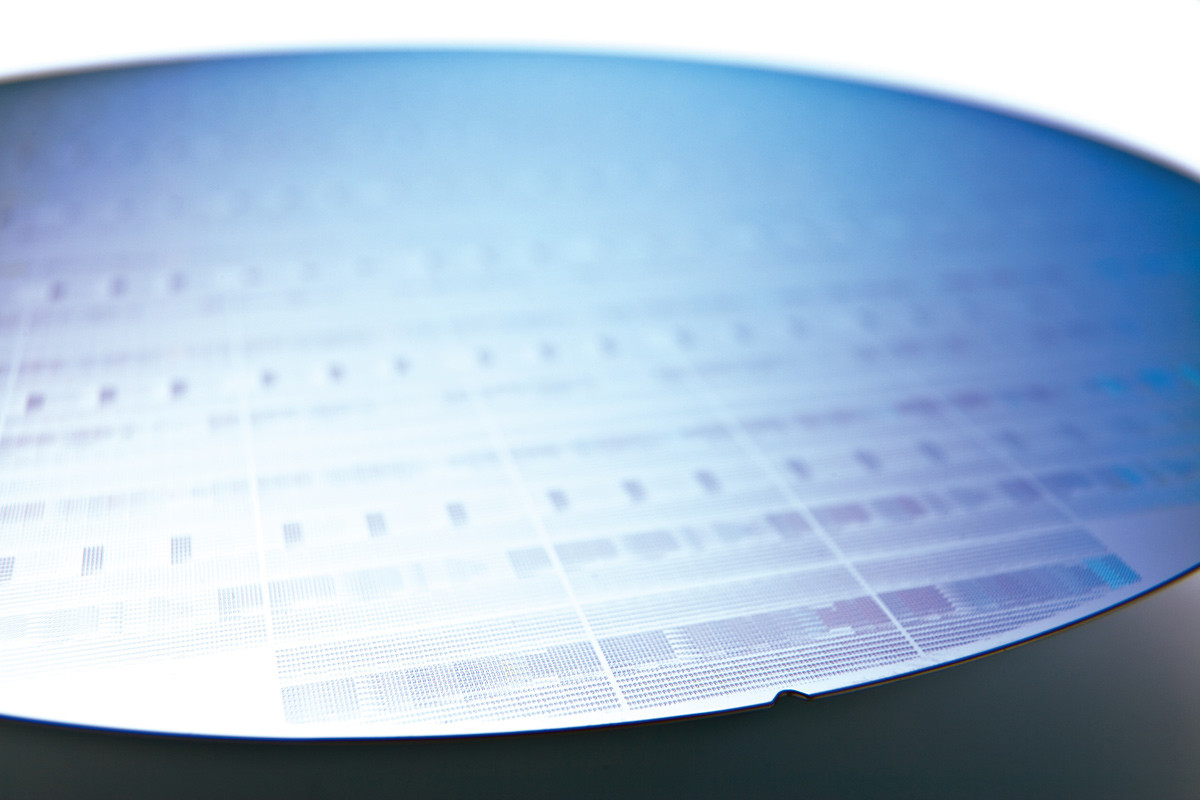
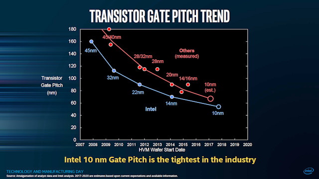
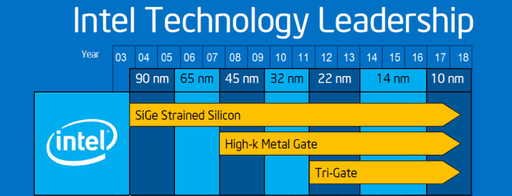
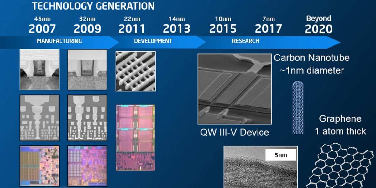
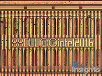
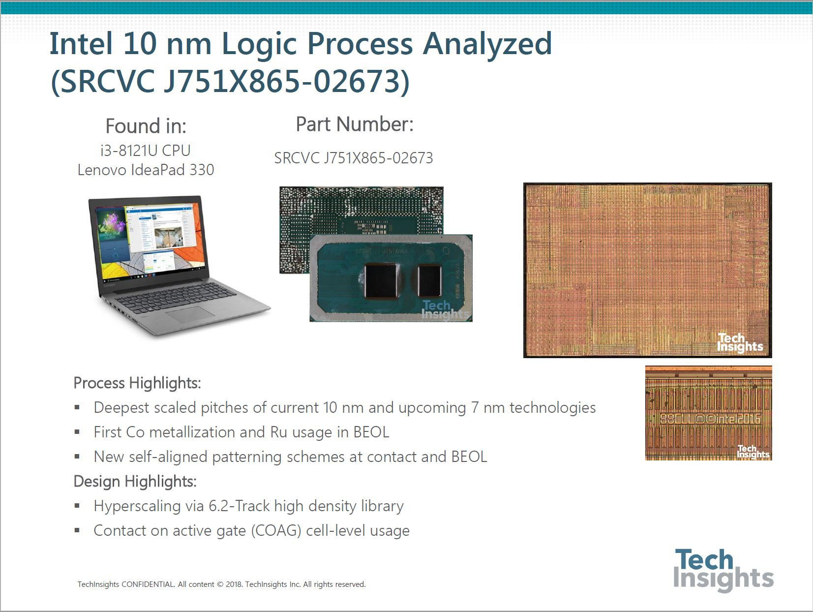
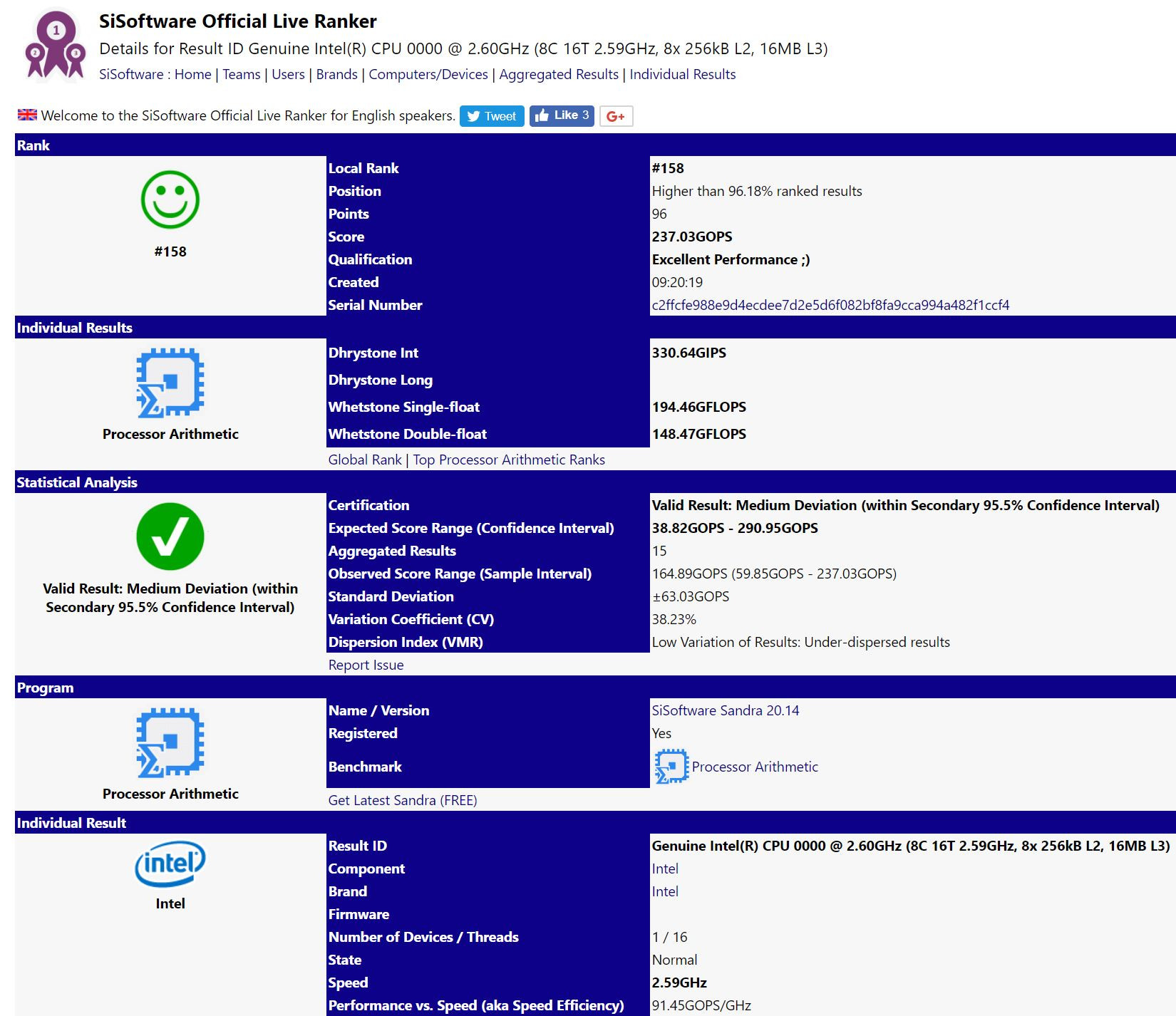
There could be light at the end of the tunnel for Intel's silicon fabrication business after all, as the company reported that its 7 nanometer silicon fabrication node, which incorporates EUV (extreme ultraviolet) lithography, is on track. The company stressed in its Nasdaq Investors' Conference presentation that its 7 nm EUV process is de-linked from its 10 nm DUV (deep ultraviolet) node, and that there are separate teams working on their development. The 10 nm DUV node is qualitatively online, and is manufacturing small batches of low-power mobile "Cannon Lake" Core processors.
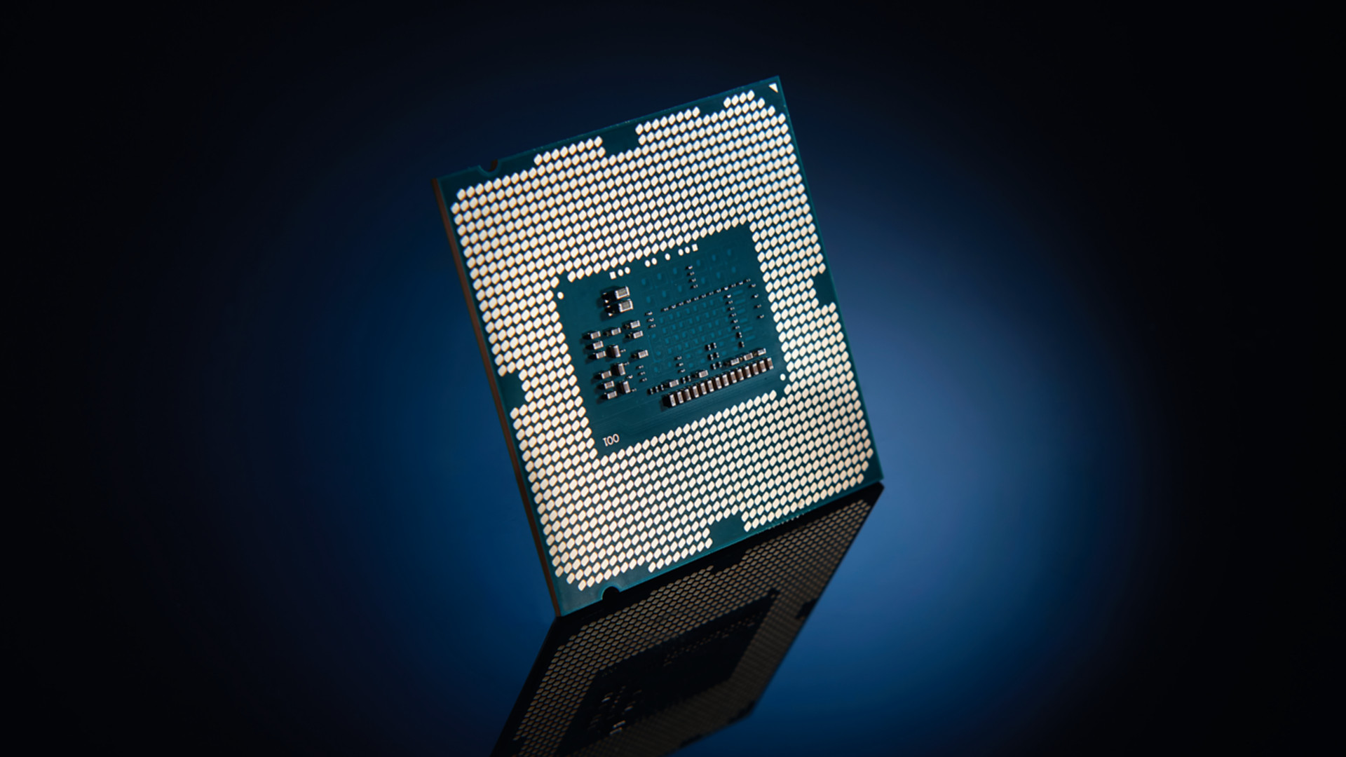
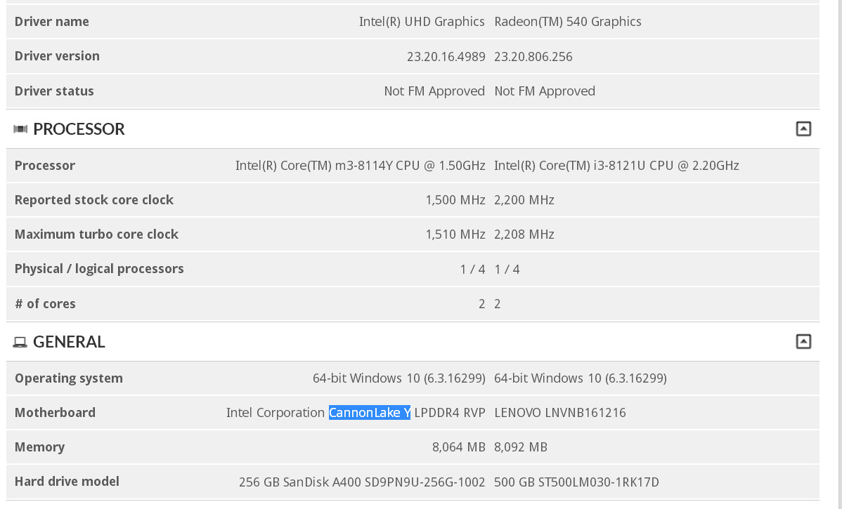
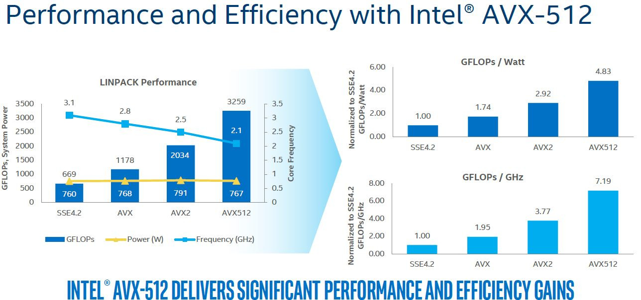
Cannon Lake is an optical shrink of the "Skylake" architecture to the 10 nm node. Currently there's only one SKU based on it, the Core i3-8121U. Intel utilized the electrical gains from the optical shrink to redesign the client-segment architecture's FPU to support the AVX-512 instruction-set (although not as feature-rich as the company's enterprise-segment "Skylake" derivatives). The jump from 10 nm DUV to 7 nm EUV will present a leap in transistor densities, with Intel expecting nothing short of a doubling. 10 nm DUV uses a combination of 193 nm wavelength ultraviolet lasers and multi-patterning to achieve its transistor density gains over 14 nm++. The 7 nm EUV node uses an extremely advanced 135 nm indirect laser, reducing the need for multi-patterning. The same laser coupled with multi-patterning could be Intel's ticket to 5 nm.
Cannon Lake is an optical shrink of the "Skylake" architecture to the 10 nm node. Currently there's only one SKU based on it, the Core i3-8121U. Intel utilized the electrical gains from the optical shrink to redesign the client-segment architecture's FPU to support the AVX-512 instruction-set (although not as feature-rich as the company's enterprise-segment "Skylake" derivatives). The jump from 10 nm DUV to 7 nm EUV will present a leap in transistor densities, with Intel expecting nothing short of a doubling. 10 nm DUV uses a combination of 193 nm wavelength ultraviolet lasers and multi-patterning to achieve its transistor density gains over 14 nm++. The 7 nm EUV node uses an extremely advanced 135 nm indirect laser, reducing the need for multi-patterning. The same laser coupled with multi-patterning could be Intel's ticket to 5 nm.