News Posts matching #Silicon

Return to Keyword Browsing

Researchers Build a CPU Without Silicon Using Carbon Nanotubes

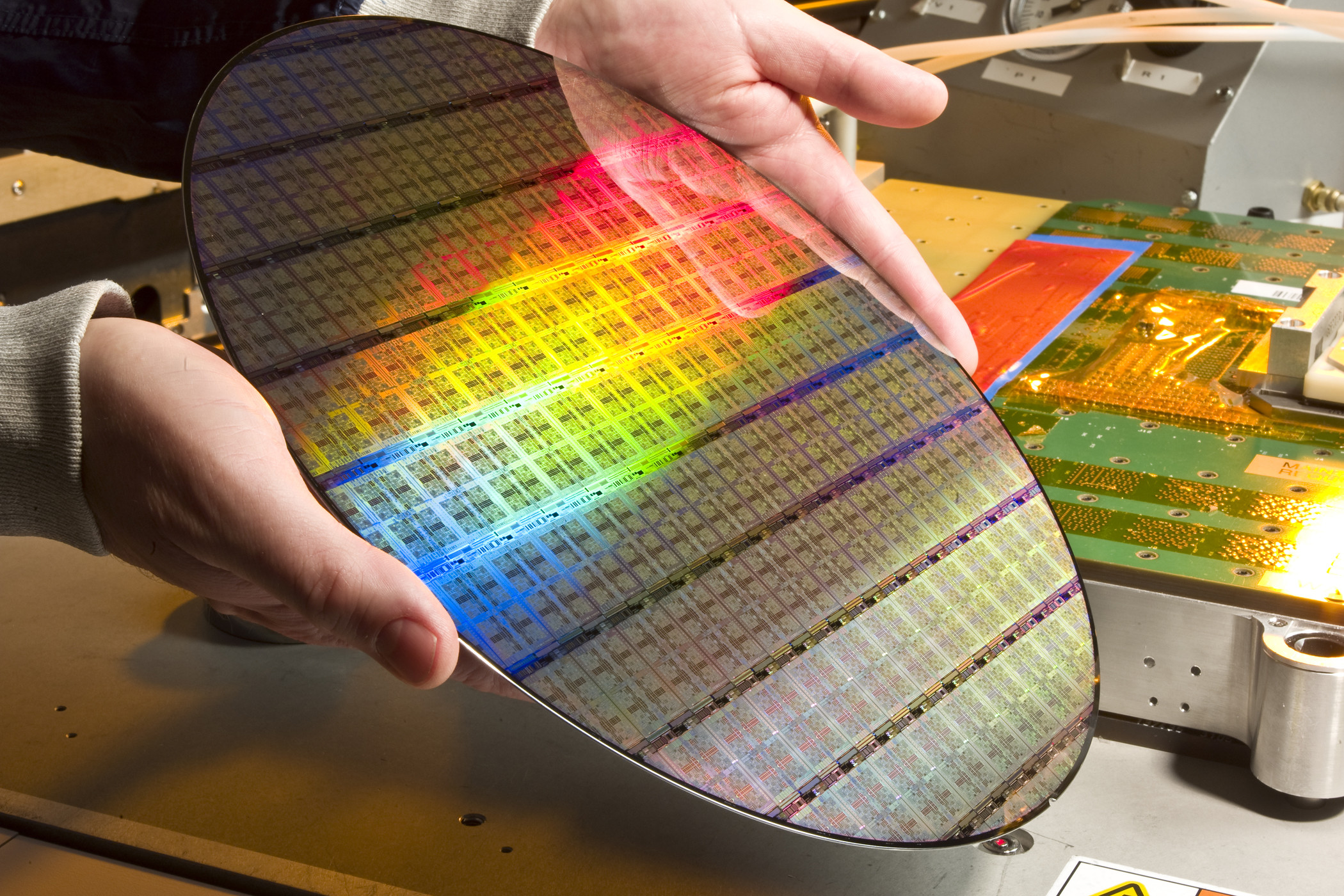
It is no secret that silicon manufacturing is an expensive and difficult process which requires big investment and a lot of effort to get right. Take Intel's 10 nm for example. It was originally planned to launch in 2015, but because of technical difficulties, it got delayed for 2019. That shows how silicon scaling is getting more difficult than ever, while costs are rising exponentially. Development of newer nodes is expected to cost billions of Dollars more, just for the research alone and that is not even including the costs for the setting up a manufacturing facility. In order to prepare for the moment when the development of ever-decreasing size nodes becomes financially and physically unfeasible, researchers are exploring new technologies that could replace and possibly possess even better electrical properties than silicon. One such material (actually a structure made from it) is Carbon Nanotube or CNT in short.

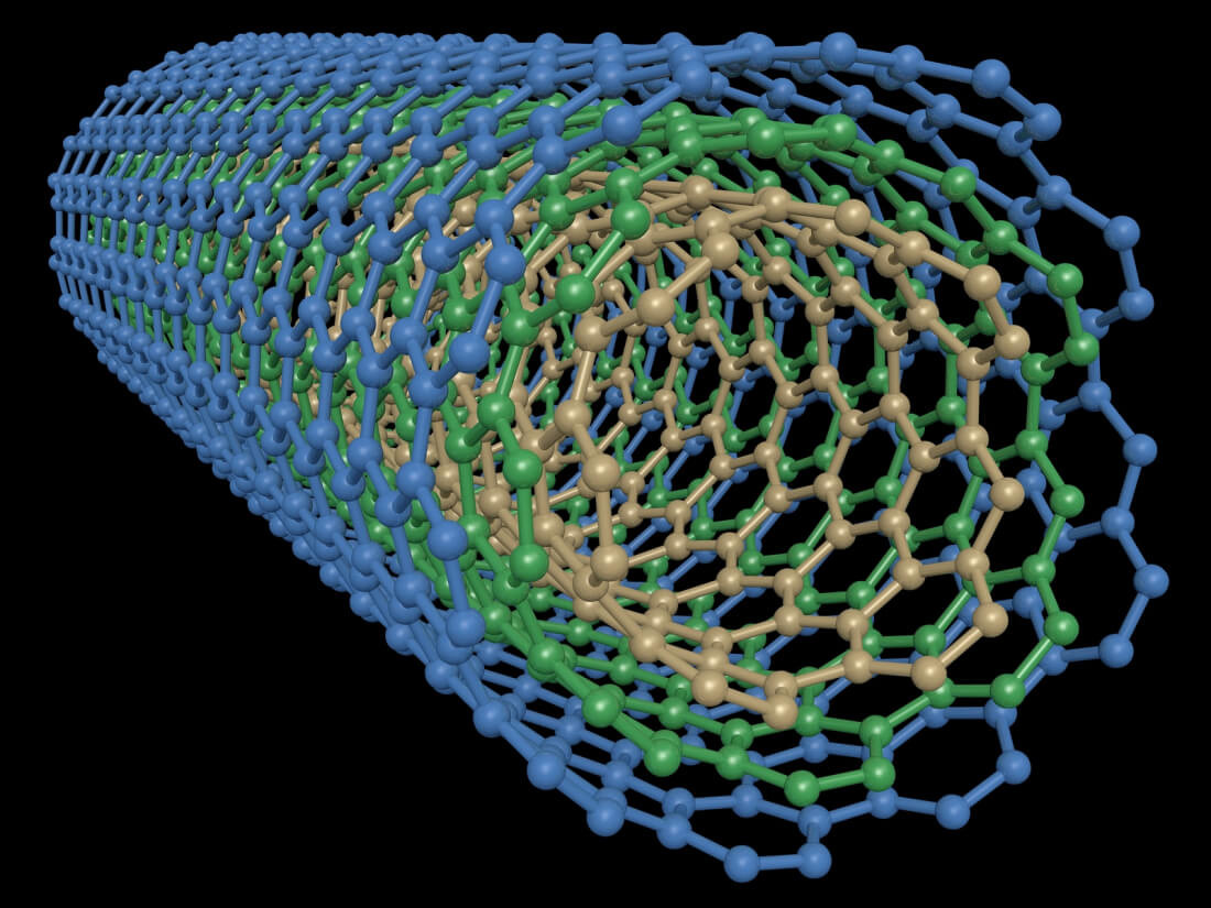
Researchers from MIT, in collaboration with scientists from Analog Devices, have successfully built a CPU based on RISC-V architecture entirely using CNTs. Called RV16X Nano, this CPU is currently only capable of executing a classic "Hello World" program. CNT is a natural semiconductor, however, when manufactured, it is being made as a metallic nanotube. That is due to the fact that metallic nanotubes are easier to integrate into the manufacturing ecosystem. Its has numerous challenges in production because CNTs tend to position themselves randomly in XYZ axes. Researchers from MIT and Analog Devices solved this problem by making large enough surfaces so that enough random tubes are positioned well.

Silicon Lottery Starts Selling Binned 3rd Generation AMD Ryzen CPUs

Silicon Lottery, a company specializing in the process called binning which involves testing of CPUs for particular features (overclocking potential in this case), has released its portfolio of 3rd generation of Ryzen CPUs. As of now, they are offering only Ryzen 7 and Ryzen 9 models, covering Ryzen 7 3700X, 3800X and Ryzen 9 3900X. Ryzen 9 3950X is said to be introduced in September and that is the date Silicon Lottery will reveal the information about overclocking potential of that model and frequencies they have achieved. Mid range Ryzen 5 models should be added at later date as well.

ARM Revokes Huawei's Chip IP Licence

As the trade war between the US and China continues to unfold, we are seeing major US companies ban or stop providing service to China's technology giant Huawei. Now, it looks like the trade war has crossed the ocean and reached the UK. This time, UK based ARM Holdings, the provider of mobile chip IP for nearly all smartphones and tablets, has revoked the license it has given Huawei.

According to the BBC, ARM Holdings employees were instructed to suspend all interactions with Huawei, and to send a note informing Huawei that "due to an unfortunate situation, they were not allowed to provide support, deliver technology (whether software, code, or other updates), engage in technical discussions, or otherwise discuss technical matters with Huawei, HiSilicon or any of the other named entities." The news came from an internal ARM document the BBC has obtained.

Intel Again Leader in Silicon Supply Race

Intel was the historic leader in silicon manufacturing and sales from 1993 through 2016, the year it lost its lead to Samsung. The issue wasn't so much to do with Intel, but more to do with market demands at the time - if you'll remember, it was the time of booming DRAM pricing alongside the smartphone demand increase that propagated stiff competition and manufacturers trying to outgun one another in the form of specs. The DRAM demand - and its ridiculous prices, at the time - propelled Samsung towards the top spot in terms of revenue, leaving Intel in the dust.

However, with the decrease in DRAM pricing following the reduce in smartphone demand and increased manufacturing capabilities of semiconductor manufacturers, which flooded the market with product that is being more slowly digested, has led to the drop of the previously-inflated Dram pricing, thus hitting Samsung's revenues enough for Intel to again become "top dog" in the silicon manufacturing world - even as the company struggles with its 10 nm rollout and faced supply issues of their own. As IC Insights puts it, "Intel replaced Samsung as the number one quarterly semiconductor supplier in 4Q18 after losing the lead spot to Samsung in 2Q17. (...) With the collapse of the DRAM and NAND flash markets over the past year, a complete switch has occurred, with Samsung having 23% more total semiconductor sales than Intel in 1Q18 but Intel having 23% more semiconductor sales than Samsung just one year later in 1Q19!".

U.S. Tech Industry, Including Google, Microsoft, Intel, and Qualcomm, Ban Huawei

The United States tech industry has overnight dealt a potentially fatal blow to Chinese electronics giant Huawei, by boycotting the company. The companies are establishing compliance with a recent Executive Order passed by President Donald Trump designed to "stop the import, sale, and use of equipment and services by foreign companies based in countries that are potential adversaries to U.S. interests," particularly information technology security. Google has announced that it will no longer allow Huawei to license Android, and will stop updates and Google Play access to Huawei smartphones. Huawei can still equip its phones with open-source Android, but it cannot use Google's proprietary software, including Google Play Store, Chrome, and all the other Google apps. Intel decided to no longer supply processors and other hardware to Huawei, for use in its laptops and server products. Sales of AMD processors will stop, too. Qualcomm-Broadcom have decided to stop supply of mobile SoCs and network PHYs, respectively. Microsoft decided to stop licensing Huawei to use Windows and Office products.

The ban is a consequence of the U.S. Government placing Huawei on a list of banned entities, forcing all U.S. companies to abandon all trade with it, without prior approval from the Department of Commerce. Trade cuts both ways, and not only are U.S. firms banned from buying from Huawei, they're also banned from selling to it. Huawei "buys from" over 30 U.S. companies, (for example, Windows licenses from Microsoft). CNN reports that U.S. firms could lose up to $11 billion in revenues.

Semiconductor Chip Sales Suffer Fourth Largest Decline in 35 Years

According to the World Semiconductor Trade Statistics (WSTS) organization, the semiconductor manufacturing world has just seen one of the largest contractions in the last 35 years. The downturn on produced revenue for manufacturers for the month of March consolidated into a decline of 1.8% compared to February of this year, and a decline of 13% when compared to March 2018 - but quarter-reviewed revenues were even worse. In greenback terms, the semiconductor industry saw a decline from $114.7 billion in the previous quarter to "just" $96.8 billion.

The decline was across all semiconductor product categories, as John Neuffer, president and CEO of the Semiconductor Industry Association (SIA) trade group, said: "Sales in March decreased on a year-to-year basis across all major regional markets and semiconductor product categories, consistent with the cyclical trend the global market has experienced recently." Market analysis firm IC Insights says that the decline was more severe than the WSTS reports, and that it totaled a 17.1% reduction in revenue for the first quarter of this year, making it the fourth biggest decline since 1984. As IC Insights said in a statement, "The first quarter is usually the weakest quarter of the year for the IC market, averaging a sequential decline of 2.1% over the past 36 years, but the severity of the 1Q19/4Q18 IC market drop has started this year off at a very low level."

TSMC Completes 5 nm Design Infrastructure, Paving the Way for Silicon Advancement

TSMC announced they've completed the infrastructure design for the 5 nm process, which is the next step in silicon evolution when it comes to density and performance. TSMC's 5 nm process will leverage the company's second implementation of EUV (Extreme Ultra Violet) technology (after it's integrated in their 7 nm process first), allowing for improved yields and performance benefits.

According to TSMC, the 5 nm process will enable up to 1.8x the logic density of their 7 nm process, a 15% clock speed gain due to process improvements alone on an example Arm Cortex-A72 core, as well as SRAM and analog circuit area reduction, which means higher number of chips per wafer. The process is being geared for mobile, internet, and high performance computing applications. TSMC also provides online tools for silicon design flow scenarios that are optimized for their 5 nm process. Risk production is already ongoing.

AMD Says Not to Count on Exotic Materials for CPUs in the Next Ten Years, Silicon Is Still Computing's Best Friend

AMD's senior VP of AMD's datacentre group Forrest Norrod, at the Rice Oil and Gas HPC conference, said that while graphene does have incredible promise for the world of computing, it likely will take some ten years before such exotic material are actually taken advantage off. As Norrod puts it, silicon still has a pretty straightforward - if increasingly complex - path down to 3 nanometer densities. And according to him, at the rate manufacturers are being able to scale down their production nodes further, the average time between node transitions stands at some four or five years - which makes the jump to 5 nm and then 3 nm look exactly some 10 years from now, where Norrod expects to go through two additional shrinking nodes for the manufacturing process.

Of course, graphene is being hailed as the next best candidate for taking over silicon's place at the heart of our more complex, high-performance electronics, due, in part, to its high conductivity independent of temperature variation and its incredible switching resistance - it has been found to be able to operate at Terahertz switching speeds. It's a 2D material, which means that implementations of it will have to occur in deposited sheets of graphene across some other material.

Capital Expenditure on Silicon Chip Manufacturing to Rise to $67.5 billion in 2019

The race for smaller fabrication processes has become more and more expensive, and the expenses in R&D and factory retooling only look to increase. This - alongside the expected increase in demand from silicon-embedded products, which are almost all of them - means that additional funding will be poured into chip manufacturing capabilities. A report from SEMI indicates that the 14% increased investment in 2018 to $62.8 billion will increase a further 7.5% next year, reaching capital expenditure of $67.5 billion in 2019.

3D NAND fabrication plants lead the charge in investment, even if the market is facing some issues stemming from oversupply. The demand growth is being taken into account for these new expansion plans, however, with denser and denser chips being required for all manner of products. This is part of the reason why 43% of this years' spending has been allotted to new NAND factories, but the ratio for 2019 is a much lower 19% increase.

Silicon Lottery Posts its Pricing of the Core i9-9900K and i7-9700K

Silicon Lottery is an online retailer that sells computer hardware its employees personally bin to pick out the best performing parts, at higher-than-MSRP prices. It listed its pricing for the upcoming Intel Core i9-9900K 8-core/16-thread processor, and the Core i7-9700K 8-core/8-thread part. The site currently reports both parts as "sold out" either because they've actually sold out all their pre-order inventory, or because they have't built inventories yet. Regardless, the i9-9900K is listed at USD $479.99, and the i7-9700K at $369.99.

We've been actively tracking down possible list prices of Intel's 9th generation Core processors. Our most recent article on the topic predicts the i9-9900K to be priced around $450, the i7-9700K at $350, and the i5-9600K at $250. Either Silicon Lottery's listings don't include any premiums, or Intel could surprise us with prices lower than our predictions.

On The Coming Chiplet Revolution and AMD's MCM Promise

With Moore's Law being pronounced as within its death throes, historic monolithic die designs are becoming increasingly expensive to manufacture. It's no secret that both AMD and NVIDIA have been exploring an MCM (Multi-Chip-Module) approach towards diverting from monolithic die designs over to a much more manageable, "chiplet" design. Essentially, AMD has achieved this in different ways with its Zen line of CPUs (two CPU modules of four cores each linked via the company's Infinity Fabric interconnect), and their own R9 and Vega graphics cards, which take another approach in packaging memory and the graphics processing die in the same silicon base - an interposer.

Q4 2017 300 mm Silicon Wafer Pricing to Increase 20% YoY in DRAM-like Squeeze

Silicon wafers are definitely the best kind of wafers for us tech enthusiasts, but as we all know, required financial resources for the development and production of these is among the most intensive in development costs and R&D. It's not just about the cost of employing enough (and crucially, good enough) engineers that can employ the right tools and knowledge to design the processing miracles that are etched onto wafers; there's also the cost of good, old production as well. Extreme Ultraviolet Lithography Systems that are used for the production of silicon wafers are about the size of a city bus, and typically cost more than 100 million euros ($115.3 million) each. ASML, a Dutch company that specializes in this kind of equipment, announced this year it was expecting to see a 25% revenue growth for 2017. Increased demand for these systems - and added cost of development of ever increasingly small and complex etchings in wafers - means this sector is seeing strong growth. But where there is strong growth, there is usually high demand, and high demand means higher strain on supply, which may sometimes not be able to keep up with the market's needs.

This is seemingly the case for wafer pricing; as demand for wafer production has been increasing, so to are prices. Faced with increased demand, companies are usually faced with a tough question to answer in regards to the correct course of action. Usually, it goes like this: higher demand at the same supply level means higher pricing. However, if supply isn't enough to satisfy demand, manufacturers are losing out on potential increased sales. This leads most companies to increase supply relative to demand, but always with lower projected output than demand requires, so they can bask in both increased ASP (Average Sale Price) and higher number of sales. This has been the case with DRAM memory production for some time now: and is happening with 300 mm silicon wafers as well.

MIT, Stanford Partner Towards Making CPU-Memory BUSes Obsolete

Graphene has been hailed for some time now as the next natural successor to silicon, today's most used medium for semiconductor technology. However, even before such more exotic solutions to current semiconductor technology are employed (and we are still way off that future, at least when it comes to mass production), engineers and researchers seem to be increasing their focus in one specific part of computing: internal communication between components.

Typically, communication between a computer's Central Processing Unit (CPU) and a system's memory (usually DRAM) have occurred through a bus, which is essentially a communication highway between data stored in the DRAM, and the data that the CPU needs to process/has just finished processing. The fastest CPU and RAM is still only as fast as the bus, and recent workloads have been increasing the amount of data to be processed (and thus transferred) by orders of magnitude. As such, engineers have been trying to figure out ways of increasing communication speed between the CPU and the memory subsystem, as it is looking increasingly likely that the next bottlenecks in HPC will come not through lack of CPU speed or memory throughput, but from a bottleneck in communication between those two.

Samsung Announces Comprehensive Process Roadmap Down to 4 nm

Samsung stands as a technology giant in the industry, with tendrils stretching out towards almost every conceivable area of consumer, prosumer, and professional markets. It is also one of the companies which can actually bring up the fight to Intel when it comes to semiconductor manufacturing, with some analysts predicting the South Korean will dethrone Intel as the top chipmaker in Q2 of this year. Samsung scales from hyper-scale data centers to the internet-of-things, and is set to lead the industry with 8nm, 7nm, 6nm, 5nm, 4nm and 18nm FD-SOI in its newest process technology roadmap. The new Samsung roadmap shows how committed the company is (and the industry with it) towards enabling the highest performance possible from the depleting potential of the silicon medium. The 4 nm "post FinFET" structure process is set to be in risk production by 2020.

This announcement also marks Samsung's reiteration on the usage of EUV (Extreme Ultra Violet) tech towards wafer manufacturing, a technology that has long been hailed as the savior of denser processes, but has been ultimately pushed out of market adoption due to its complexity. Kelvin Low, senior director of foundry marketing at Samsung, said that the "magic number" for productivity (as in, with a sustainable investment/return ratio) with EUV is 1,500 wafers per day. Samsung has already exceeded 1,000 wafers per day and has a high degree of confidence that 1,500 wafers per day is achievable.

GlobalFoundries Announces its 12 nm FD-SOI Silicon Fabrication Node

GLOBALFOUNDRIES today unveiled a new 12nm FD-SOI semiconductor technology, extending its leadership position by offering the industry's first multi-node FD-SOI roadmap. Building on the success of its 22FDXTM offering, the company's next-generation 12FDXTM platform is designed to enable the intelligent systems of tomorrow across a range of applications, from mobile computing and 5G connectivity to artificial intelligence and autonomous vehicles.

As the world becomes more and more integrated through billions of connected devices, many emerging applications demand a new approach to semiconductor innovation. The chips that make these applications possible are evolving into mini-systems, with increased integration of intelligent components including wireless connectivity, non-volatile memory, and power management-all while driving ultra-low power consumption. GLOBALFOUNDRIES' new 12FDX technology is specifically architected to deliver these unprecedented levels of system integration, design flexibility, and power scaling.

Intel Core i7-6950X Tested Against i7-5960X

Silicon Lottery at OCN got their hands on Intel's upcoming flagship high-end desktop (HEDT) processor, the Core i7-6950X. Based on the 14 nm "Broadwell-E" silicon, the processor offers a staggering 10 cores, with HyperThreading enabling 20 logical CPUs, 25 MB L3 cache, and a quad-channel DDR4 memory controller. The i7-6950X is expected to occupy a price point that's above the $999 traditionally reserved for the top-end HEDT chip. Silicon Lottery successfully overclocked the i7-6950X to 4.50 GHz, from its rumored stock frequency of 3.00 GHz, and compared it to a previous-generation Core i7-5960X 8-core processor. The common platform consisted of an ASUS Rampage V Extreme motherboard, 16 GB of quad-channel DDR4-3000 memory, and GeForce GTX 750 Ti graphics.

At its top overclock of 4.50 GHz, the i7-6950X achieved a Cinebench R15 score of 2327 points. At 4.00 GHz, it scored 1904 points, 19.5 percent higher than the i7-5960X at the same clocks (the i7-6950X features two extra cores). The two chips were also put through AIDA64 memory tests. The memory read speeds were nearly the same, but the memory write speeds were found to be a staggering 37 percent higher on the i7-6950X. The memory copy speeds, however, were 10.5 percent lower on the i7-6950X. Intel is expected to launch its next-generation Core i7 HEDT lineup, including two six-core, one eight-core, and one ten-core chips, in a few weeks from now.

NVIDIA GeForce GTX 980 Ti Silicon Marked "GM200-310"

NVIDIA's upcoming high-end single-GPU graphics card, based on the GM200 silicon, which debuted with the GTX TITAN X, will feature a silicon marked "GM200-310." The SKU will be named GeForce GTX 980 Ti, and is more likely to be priced around the $600-650 mark, than replacing the $550 GTX 980 off the shelves. Going by the way NVIDIA re-positioned the GTX 780 to $499 with the introduction of the GTX 780 Ti, we imagine something similar could happen to the GTX 980. From what we gathered so far, the GTX 980 Ti will be based on the GM200 silicon. Its CUDA core count is unknown, but it wouldn't surprise us if it's unchanged from the GTX TITAN X. Its different SKU numbering shouldn't be an indication of its CUDA core count. GTX 780 Ti and GTX TITAN Black had different numbering, but the same CUDA core counts of 2,880.

The card will feature 6 GB of GDDR5 memory across the chip's 384-bit wide memory interface. It will feature five display outputs, similar to that of the GTX 980. Unlike with the GTX TITAN X, NVIDIA partners will have the freedom to launch custom-design GTX 980 Ti products from day-one. There are two theories doing rounds on when NVIDIA plans to launch this card. One suggests that it could launch in mere weeks from now, probably even on the sidelines of Computex. The other suggests that it will launch towards the end of Summer, as NVIDIA wants to make the most cash from its existing GTX 980 inventory.

IDF 2013 Transforming Computing Experiences from the Device to the Cloud

During her keynote at the Intel Developer Forum today in Beijing, Diane Bryant, senior vice president and general manager of Intel's Datacenter and Connected Systems Group, discussed how her company is helping users harness powerful new capabilities that will improve the lives of people by building smarter cities, healthier communities and thriving businesses.

Bryant unveiled details of upcoming technologies and products that show how Intel aims to transform the server, networking and storage capabilities of the datacenter. By addressing the full spectrum of workload demands and providing new levels of application optimized solutions for enterprise IT, technical computing and cloud service providers, unprecedented experiences can be delivered.

IBM Lights Up Silicon Chips to Tackle Big Data

IBM announced today a major advance in the ability to use light instead of electrical signals to transmit information for future computing. The breakthrough technology - called "silicon nanophotonics" - allows the integration of different optical components side-by-side with electrical circuits on a single silicon chip using, for the first time, sub-100 nm semiconductor technology.

Silicon nanophotonics takes advantage of pulses of light for communication and provides a super highway for large volumes of data to move at rapid speeds between computer chips in servers, large datacenters, and supercomputers, thus alleviating the limitations of congested data traffic and high-cost traditional interconnects.

TSMC Tapes Out CoWoS Test Vehicle Integrating Wide I/O Mobile DRAM Interface

TSMC today announced that it has taped out the foundry segment's first CoWoS (Chip on Wafer on Substrate) test vehicle using JEDEC Solid State Technology Association's Wide I/O mobile DRAM interface. The milestone demonstrates the industry's system integration trend to achieve increased bandwidth, higher performance and superior energy efficiency.

This new generation of TSMC's CoWoS test vehicles added a silicon proof point demonstrating the integration of a logic SoC chip and DRAM into a single module using the Wide I/O interface. TSMC's CoWoS technology provides the front-end manufacturing through chip on wafer bonding process before forming the final component. Along with Wide I/O mobile DRAM, the integrated chips provide optimized system performance and a smaller form factor with significantly improved die-to-die connectivity bandwidth.

Intel and ASML Reach Agreements to Accelerate Key Next-Generation Silicon Fab Tech

Intel Corporation today announced it has entered into a series of agreements with ASML Holding N.V. intended to accelerate the development of 450-millimeter (mm) wafer technology and extreme ultra-violet (EUV) lithography totaling €3.3 billion (approximately $4.1 billion). The objective is to shorten the schedule for deploying the lithography equipment supporting these technologies by as much as two years, resulting in significant cost savings and other productivity improvements for semiconductor manufacturers.

To achieve this, Intel is participating in a multi-party development program that includes a cash contribution by Intel to fund relevant ASML research and development (R&D) efforts as well as equity investments in ASML. The first phase of this program consists of Intel committing to R&D funding of €553 million (approximately $680 million) to assist ASML in accelerating the development and delivery of 450-mm manufacturing tools, as well as an equity investment of €1.7 billion (approximately $2.1 billion) for approximately 10 percent of ASML's pre-transaction issued shares. Intel will record the R&D investment as a combination of R&D expense and pre-payments on future tool deliveries.

GLOBALFOUNDRIES Improves IC Reliability with Customized Circuit Checks

Mentor Graphics Corp. today announced that GLOBALFOUNDRIES is helping its customers improve reliability checking by adding Calibre PERC to select 28nm bulk CMOS design enablement flows. Calibre PERC will give designers access to the new reliability verification rules developed by the IBM Semiconductor Development Alliance (ISDA), augmented with GLOBALFOUNDRIES specific checks to help prevent external latch-up. Using Calibre PERC's unique architecture, complex reliability rules that require the integration of logical (net list) and layout (GDS) information can be fully automated, eliminating manual spreadsheet-based efforts and reducing the chances of design errors.

"In the past, verification of latch-up immunity depended on manual layout checks and rough approximations of device and interconnect resistance using traditional mechanisms," said Bill Liu, vice president of design enablement at GLOBALFOUNDRIES. "Now our customers can perform accurate measurements and analysis automatically using Calibre PERC's data integration capability. For example, some of our customers are currently using PERC to accurately determine the resistance of the paths in complex output driver arrays as a function of device spacing. This allows them to easily and accurately detect points in the circuit where latch-up could be an issue and to make appropriate improvements."

GLOBALFOUNDRIES Fab 8 Adds Tools to Enable 3D Chip Stacking at 20nm and Beyond

GLOBALFOUNDRIES today announced a significant milestone on the road to enabling 3D stacking of chips for next-generation mobile and consumer applications. At its Fab 8 campus in Saratoga County, NY, the company has begun installation of a special set of production tools to create Through-Silicon Vias (TSVs) in semiconductor wafers processed on the company's leading-edge 20nm technology platform. The TSV capabilities will allow customers to stack multiple chips on top of each other, providing another avenue for delivering the demanding requirements of tomorrow's electronic devices.

Essentially vertical holes etched in silicon and filled with copper, TSVs enable communication between vertically stacked integrated circuits. For example, the technology could allow circuit designers to place stacks of memory chips on top of an application processor, which can dramatically increase memory bandwidth and reduce power consumption-a key challenge for designers of the next generation of mobile devices such as smartphones and tablets.

Biwin America, Inc. Founded to Develop Advanced New SSD Storage Solutions

Biwin today announced the opening of Biwin America, Inc., in San Jose, California to develop and market new flash based SSD storage solutions for enterprise, embedded and client applications.

Biwin is already an established leader in OEM and ODM USB flash drives. The company boasts impressive manufacturing strength that includes die sorting and packaging, over 20 SMT lines, and sophisticated test and QC processes. The founding of Biwin America, Inc., in the heart of Silicon Valley, marks the company's expansion into the USA market with a focus on expanding their existing SSD product portfolio. The company will sell its products directly to OEMs as well as through distribution.

Common Platform Transitions to Adopt FinFET 3D Transistor with 14 nm Fab Process

Common Platform, a consortium of three major silicon fabrication companies: IBM, Samsung, and GlobalFoundries, met at their 2012 Technology Forum, where they announced their intention to transition to FinFET 3D transistor technology, but only with the 14 nanometer (nm) silicon fabrication process. Chips on this process will be built in the 2014~2015 time-frame. 3D transistors is a technology pioneered by Intel, which provides space-optimized, energy-efficient transistors on a nano-scale.

FinFET transistors will be combined with Fully Depleted Silicon-On-Insulator (FD-SOI) to offer extremely high transistor densities, with lower chip power. FD-SOI overcomes the limitation of current partially-depleted SOI (PD-SOI) technology, of lower-yields due to the pressure required for SOI insulation, which nears the breaking-point of strained silicon transistors. FinFET tech will be combined with chip-stacking technology, which helps make devices with better use of available PCB footprint.
Return to Keyword Browsing
Jul 12th, 2025 07:21 CDT change timezone

New Forum Posts

Popular Reviews

TPU on YouTube

Controversial News Posts