Tuesday, September 4th 2018

Analyst Firm Susquehanna: "Intel Lost its Manufacturing Leadership"
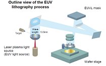
Intel was once the shining star in the semiconductor manufacturing industry, with a perfectly integrated, vertical product design and manufacturing scheme. Intel was one of the few companies in the world to be able to both develop its architectures and gear their manufacturing facilities to their design characteristics, ensuring a perfect marriage of design and manufacturing. However, not all is rosy on that field, as we've seen; AMD itself also was a fully integrated company, but decided to spin-off its manufacturing arm so as to survive - thus creating GLOBALFOUNDRIES.But Intel was seen as many as the leader in semiconductor manufacturing, always at the cutting edge of - well - Moore's Law, named after Intel's founding father Gordon Moore. Now, Mehdi Hosseini, an analyst with Susquehanna, has gone on to say that the blue giant has effectively lost its semiconductor leadership. And it has, in a way, even if its 10 nm (which is in development hell, so to speak) is technically more advanced than some 7 nm implementations waiting to be delivered to market by its competitors. However, there's one area where Intel will stop being able to claim leadership: manufacturing techniques involving EUV (Extreme UltraViolet).It's being reported that intel has decided to postpone its EUV efforts to other processes, not taking it up on its 7 nm process development. This saves Intel money in adding yet another technique and technology to an already hard to manufacture node, but leaves the door ajar for the likes of TSMC and Samsung (of which the latter is expected to have the more complex EUV implementation, in more layers, at least in the beginning). TSMC is looking to develop both 7 nm and 7 nm+ manufacturing processes, where only the latter will feature EUV integration - a way to divide costs and reduce reliance on a still exotic technology. But while Samsung and TSMC are both looking towards some level of EUV integration by 2019, intel is looking towards a farther 2021.According to Susquehanna's Mehdi Hosseini, TSMC is the company to look out for as the semiconductor manufacturer leader, as it "appears to be winning most of the leading-edge design wins due to better 7nm process technology performance, lower power consumption and better area density." Indeed "the times, they are a changin'."
Source:
EETimes


61 Comments on Analyst Firm Susquehanna: "Intel Lost its Manufacturing Leadership"
Basically, Intel is willingly giving up on EUV and will pursue other avenues of manufacture. That leaves TSMC and Samsung. GloFo (Global Foundries) left or gave up on 7nm EUV (which they were a partner with Samsung). In my opinion, GloFo was seeing that industry leaders were not happy with their and Samsung's 7nm 8-to-10 layer EUV process and decided to ditch the 7nm process altogether.
Samsung's design is aggressive since their 7nm requires EUV and 8-to-10 layers and will, supposedly, arrive after TSMC's 7nm non-EUV. This is backfiring on them but they are still willing to push through (even at the cost of alienation). The costs are high (which have to be passed on).
TSMC will have 7nm non-EUV and 7nm+ EUV with the former arriving before Samsung's 7nm EUV process and the latter arriving after Samsung's 7nm EUV process. Industry experts are saying having flexibility with both types is an advantage, according to Mehdi Hosseini (the analyst from Susquehanna).
IPC won't change if you only change from 14nm to 10nm, for example. It usually does though when that happens, because at least some minor changes are made to the design, and it might clock higher too. 65nm and 45nm Core 2 Duo/Quad was a good example of this.
I guess there is no penalty to just use numbers for marketing purposes when billions are involved. If only intel would have said that their 10nm tech it's actually 7nm, nobody would have bat an eye.
And about the dude not knowing the industry he's just been doing this for more than ten years, plus he worked at NSC and he has an MS in electrical engineering. I rather take his word for it than some random internet dudes.
Going to a smaller node, we should expect lower clocks (at least in the first revision).
Intel, on the other hand, takes care of high clocks from the start, because that's how they differentiate the lineup. I think this is one of the reasons why 10nm is so delayed. They need it to hit near 5GHz boost from the start, or they won't be able to build a typical Intel-ish lineup.
it sad that global foundaries spended billions $ in this 7nm and buy 2 ASML buses of it and now just stop it all
can someone expert explain what is quantum problems and why it so much harder to go smaller into 7nm ?
Oof~
By 10nm++ FinFET from Intel, Samsung will be ramping up 3nm GAA EUV. TSMC's 3nm Fab($20B) won't be up and running at worst till 2022.
7nm FinFET 1H2018
7nm FinFET Plus 2H2018
5nm FinFET 2H2019
3nm ___ sometime 2022
They aren't jumping, but their 7nm is short-lived.
www.tsmc.com/english/dedicatedFoundry/technology/5nm.htm
"It is scheduled to start risk production in the second half of 2019."
In their MPW it points to mass-start(risk) for 7nm FinFETs at TSMC.
www.zgcicc.com/mpw/2018TSMCCyberShuttleServicePlan.pdf
7nm FinFET tape-in => Mar-26 2018
7nm FinFET plus tape-in => Aug-15 2018
etc.
Risk production for Samsung is when MPWs start. The same is for GlobalFoundries.
So, Samsung at least has a two year lead on TSMC. Since, the 3nm Fab for TSMC doesn't get finished till end of 2021/early 2022.
There are different quantum effects making problems in transistors, but IMO the easiest one to understand is quantum tunneling (or at least the general idea).
I'll skip the whole probability theory, waves, potentials and so on...
Basically, you have to remember that the world around you is not corpuscular (solid, made of small particles that collide). It's made of interacting "points".
In other words: particles are points (no size), but since they repel each other, they create a structure which has dimensions (just like a triangle is defined by 3 points).
So you have your typical macro-scale wire and there's an electric current inside, like this:
-----------------------------------------
outside....inside....outside
-----------------------------------------
............|-|....e....|-|................
-----------------------------------------
It's isolated by some walls |-|, so you can hold it and so on. In the scale you're looking at them with naked eye, they seem solid.
But as you zoom to nanometres (e.g. single transistors), the walls can't be treated as solid anymore.
Particles that create the walls repel electrons inside, but - as the walls become thinner and thinner - repelling becomes weak. As a result, sometimes an electron gets through the wall. :)
In other words: if you could "measure electricity" on a nano scale, you would also get some reading outside the walls as well:
-----------------------------------------------------------------------
outside.........wall.........inside........wall........outside
-----------------------------------------------------------------------
........e'........|----------|........e........|----------|......e'.......
-----------------------------------------------------------------------
:)
if I understand right, it meens that the walls insulator have to be small so that you can put many transistors and less insulators into the chip
but despite the insulator is not-conductive, the electrons flow through them anyway - not because they are not-conductive (which don't exist) - but because they are very few and very small
you meen to say it crates an effect like a static charge: 10,000 volts of static still attract each other through air at distance of 10 cm - air which is not conductive
so when this things are so littel - the problem become mutch worse, and that charge is not static
but then because electrons are flowing through the walls, they destroy the walls !
I understand now I think, there is no material in the world that can be non-conductive when he is so littel :x
so this meens, the more space you spend on insulator, the less space you have for everything :x
is this how they do QA on processor logics ? they test them for "short circuits" ?
what about making the other sides of the wall charged such that there is no differential potential so the electron don't wanne flow towards outside the wall ?
There's no reason to believe that AMD can't hit 5GHz with Zen 2 on the 7nm process. We don't have any idea what it might or might not do. Though moving to a smaller process resulting in lower clocks seems completely bonkers, at least if it's a simple die shrink with maybe a few tweaks here and there (like Wolfdale was to Conroe). I could see that happening if while moving to a smaller process you also developed a radically different architecture, like the Core 2 Duo was to the Pentium, though late Pentiums and early C2D were both 65nm.
To lose $10 a share... Ouch. Investors aren't happy with Intel right now, that's for sure.
Even 7nm, I think we will see some bumps in the road for, still.
The bottom line with roadmaps is that you can put 'progress and leadership in X' on top of a powerpoint slide so you can snag some investors and keep your stock afloat.