Monday, August 14th 2023

AMD "Navi 4C" GPU Detailed: Shader Engines are their own Chiplets
"Navi 4C" is a future high-end GPU from AMD that will likely not see the light of day, as the company is pivoting away from the high-end GPU segment with its next RDNA4 generation. For AMD to continue investing in the development of this GPU, the gaming graphics card segment should have posted better sales, especially in the high-end, which it didn't. Moore's Law is Dead scored details of what could have been a fascinating technological endeavor for AMD, in building a highly disaggregated GPU.
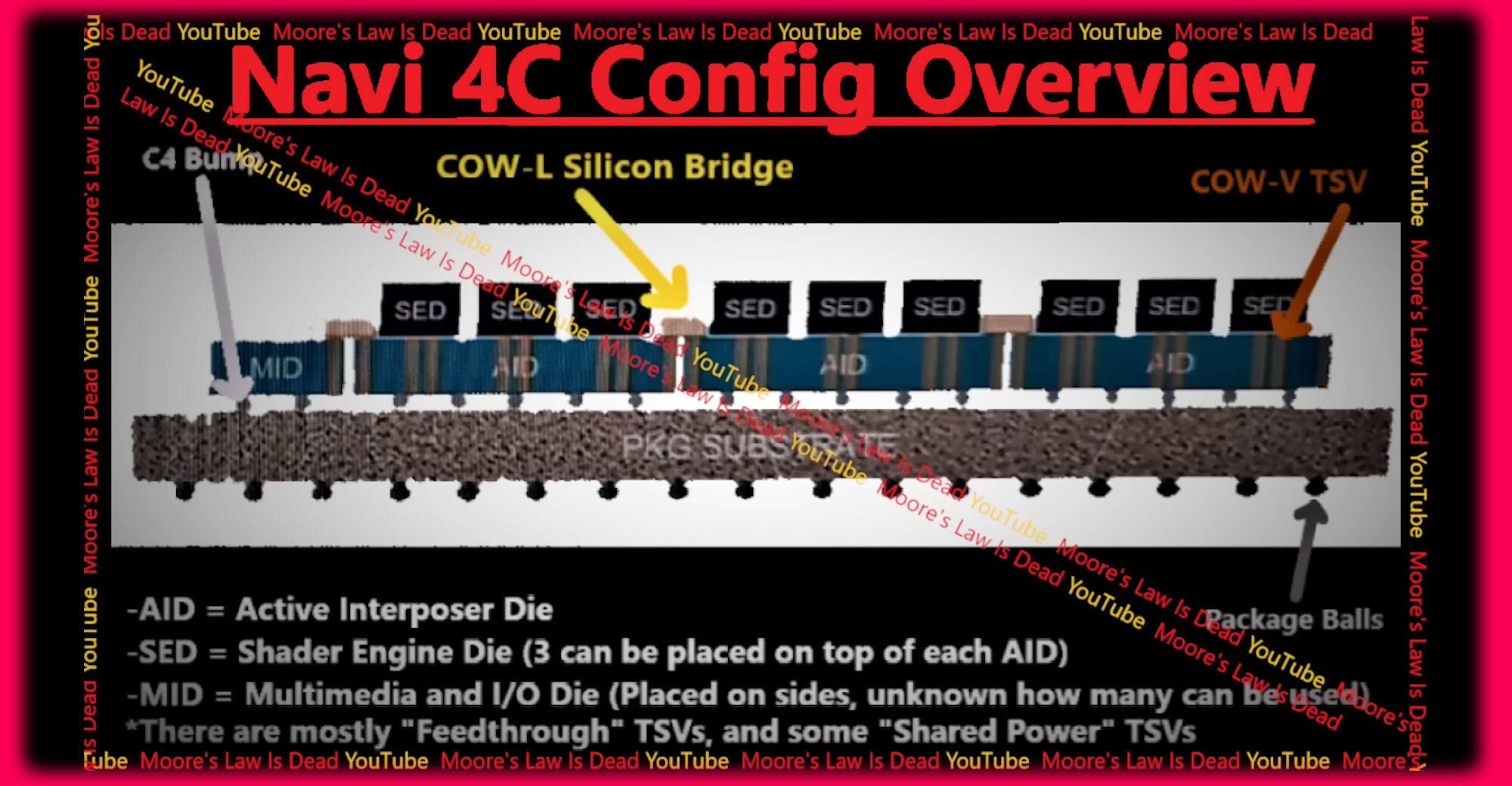
AMD's current "Navi 31" GPU sees a disaggregation of the main logic components of the GPU that benefit from the latest 5 nm foundry node to be located in a central Graphics Compute Die; surrounded by up to six little chiplets built on the older 6 nm foundry node, which contain segments of the GPU's Infinity Cache memory, and its memory interface—hence the name memory cache die. With "Navi 4C," AMD had intended to further disaggregate the GPU, identifying even more components on the GCD that can be spun out into chiplets; as well as breaking up the shader engines themselves into smaller self-contained chiplets (smaller dies == greater yields and lower foundry costs). The way AMD would go about creating "Navi 4C" would be using a vast array of packaging innovations that ensure the numerous kinds of chiplets talk to each other with as little latency as possible, as if they were parts of a whole monolithic die.
Assuming AMD had continued to use GDDR6 and not the newer GDDR7 memory standard, the company would have likely retained 6 nm MCDs from the current generation, to provide video memory interface and last-level cache to the GPU, minimizing R&D costs, and gaining from the further reduced foundry costs for the 6 nm node.
AMD identified the GPU's media acceleration engine, and Radiance Display Engine ripe for the next round of disaggregation. Although media acceleration engines are logic components, these are fixed function hardware, as are the display engines; and can likely make do with older foundry nodes. The media acceleration and display engine would be spun off into a separate chiplet called MID (media and I/O die). At this point we don't know if AMD would've gone with 6 nm or a newer node for the MID, but given that the company is able to pack the latest media and display I/O features onto the 6 nm "Navi 33" monolithic silicon, it's possible that the company would go with the older node.
Much of the semiconductor engineering muscle is centered on what happens to the most critical number-crunching machinery of the GPU, the Shader Engines. Apparently, AMD figured out that each Shader Engine, consisting of a fixed number of workgroup processors (WGPs), could be spun out into chiplets, called SEDs (shader engine dies). These would be built on an advanced foundry node. Given that NVIDIA is building its next-gen "Blackwell" GPUs on 3 nm, it's quite possible that AMD uses the same node for the SEDs.
The SEDs are seated on active interposer dies (AIDs). An interposer in general, is a silicon die whose sole purpose is to facilitate high-density microscopic wiring between chiplets stacked on top of it, with wiring densities that otherwise wouldn't be possible through fiberglass substrate. The "active" part of the AID refers to the ability of the interposer not just to facilitate wiring among dies stacked on top and to the substrate below, but also neighboring AIDs. For this purpose, TSMC innovated the COW-L (chip-on-wafer-L) bridges.
These are tiny silicon dies designed for inter-AID high-density wiring, and is how a mesh of AIDs talk to each other, and to the MID. As for how they communicate with the MCDs, remains to be seen. The current generation of MCDs are connected with the GCD using Infinity Fan-out Links—a high-density wiring method that makes do with the fiberglass substrate as the medium, instead of silicon. Should AMD be using another method to connect the MCDs, it would mean that the company is using a newer generation of them. Besides COW-L bridges, AMD is also leveraging TSMC's COW-V TSVs (through-silicon via) innovations for connecting the SEDs to the package substrate (for power and other I/O).
Alas, it's highly unlikely that "Navi 4C" will ever get off the drawing board. AMD has already implemented many of these packaging innovations with its latest MI300 compute processor based on the CDNA3 architecture, and it would have been incredible to see them in the gaming graphics segment, however, basic economics prevent AMD from investing in further development of the "Navi 4C." The gaming graphics card market is in its biggest slump since the late 2010s, and the enthusiast-class GPU caters to a niche market.
The current market conditions are a far cry from 2021, when the crypto-currency mining gold-rush had incentivized GPU manufacturers to make bigger GPUs. AMD is rumored to have mistimed the launch of its RX 6950 XT GPU toward the tail-end of the crypto boom. By that point, "Navi 31" had reached an advanced level of development and was ready to enter mass-production. The company now probably finds itself unable to justify the cost of development for "Navi 4C" beyond the concepts in this article, unless the market undergoes another dramatic upsurge in demand at the high-end.
Sources:
Moore's Law is Dead (YouTube), VideoCardz
AMD's current "Navi 31" GPU sees a disaggregation of the main logic components of the GPU that benefit from the latest 5 nm foundry node to be located in a central Graphics Compute Die; surrounded by up to six little chiplets built on the older 6 nm foundry node, which contain segments of the GPU's Infinity Cache memory, and its memory interface—hence the name memory cache die. With "Navi 4C," AMD had intended to further disaggregate the GPU, identifying even more components on the GCD that can be spun out into chiplets; as well as breaking up the shader engines themselves into smaller self-contained chiplets (smaller dies == greater yields and lower foundry costs).
Assuming AMD had continued to use GDDR6 and not the newer GDDR7 memory standard, the company would have likely retained 6 nm MCDs from the current generation, to provide video memory interface and last-level cache to the GPU, minimizing R&D costs, and gaining from the further reduced foundry costs for the 6 nm node.
AMD identified the GPU's media acceleration engine, and Radiance Display Engine ripe for the next round of disaggregation. Although media acceleration engines are logic components, these are fixed function hardware, as are the display engines; and can likely make do with older foundry nodes. The media acceleration and display engine would be spun off into a separate chiplet called MID (media and I/O die). At this point we don't know if AMD would've gone with 6 nm or a newer node for the MID, but given that the company is able to pack the latest media and display I/O features onto the 6 nm "Navi 33" monolithic silicon, it's possible that the company would go with the older node.
Much of the semiconductor engineering muscle is centered on what happens to the most critical number-crunching machinery of the GPU, the Shader Engines. Apparently, AMD figured out that each Shader Engine, consisting of a fixed number of workgroup processors (WGPs), could be spun out into chiplets, called SEDs (shader engine dies). These would be built on an advanced foundry node. Given that NVIDIA is building its next-gen "Blackwell" GPUs on 3 nm, it's quite possible that AMD uses the same node for the SEDs.
The SEDs are seated on active interposer dies (AIDs). An interposer in general, is a silicon die whose sole purpose is to facilitate high-density microscopic wiring between chiplets stacked on top of it, with wiring densities that otherwise wouldn't be possible through fiberglass substrate. The "active" part of the AID refers to the ability of the interposer not just to facilitate wiring among dies stacked on top and to the substrate below, but also neighboring AIDs. For this purpose, TSMC innovated the COW-L (chip-on-wafer-L) bridges.
These are tiny silicon dies designed for inter-AID high-density wiring, and is how a mesh of AIDs talk to each other, and to the MID. As for how they communicate with the MCDs, remains to be seen. The current generation of MCDs are connected with the GCD using Infinity Fan-out Links—a high-density wiring method that makes do with the fiberglass substrate as the medium, instead of silicon. Should AMD be using another method to connect the MCDs, it would mean that the company is using a newer generation of them. Besides COW-L bridges, AMD is also leveraging TSMC's COW-V TSVs (through-silicon via) innovations for connecting the SEDs to the package substrate (for power and other I/O).
Alas, it's highly unlikely that "Navi 4C" will ever get off the drawing board. AMD has already implemented many of these packaging innovations with its latest MI300 compute processor based on the CDNA3 architecture, and it would have been incredible to see them in the gaming graphics segment, however, basic economics prevent AMD from investing in further development of the "Navi 4C." The gaming graphics card market is in its biggest slump since the late 2010s, and the enthusiast-class GPU caters to a niche market.
The current market conditions are a far cry from 2021, when the crypto-currency mining gold-rush had incentivized GPU manufacturers to make bigger GPUs. AMD is rumored to have mistimed the launch of its RX 6950 XT GPU toward the tail-end of the crypto boom. By that point, "Navi 31" had reached an advanced level of development and was ready to enter mass-production. The company now probably finds itself unable to justify the cost of development for "Navi 4C" beyond the concepts in this article, unless the market undergoes another dramatic upsurge in demand at the high-end.
33 Comments on AMD "Navi 4C" GPU Detailed: Shader Engines are their own Chiplets
Ever since Kepler, x80 cards have mainly been using small x04 dies, between 300-400 mm2. The 2080 actually used a big 104 die that was 545 mm2 (because they added RT and tensor cores).
The 3080 used a slightly cut down 102 die, which is what made it such a great value card, one of the best in NVIDIA's history.
And there's no way the 4090 should be the 4080. But at $1200, the 4080 should be using a cut down 102 die. The 103 die should be the 104 die in the 4070/Ti. And the 104 die should be the 106 die for the 4060/Ti.
What changed with Turing is that they started releasing the 102 die right away, instead of a year later. But it's still a huge die with crazy performance. The shift actually happened with Kepler, because that's when they started using a mid-range chip in a high-end product. That was after the failure of the GTX 280 and 480, which used huge and power hungry chips with poor performance.
2080 - 9% faster than 1080 Ti
1080 - 31% faster than 980 Ti
980 - 11% faster than 780 Ti
680 - 23% faster than 580
So yes, the improvement over the previous flagship was the smallest, but it had to happen because of RTX. They had to sacrifice raster performance improvement to include RT, and that's the generation they decided to do it.
It was kind of a failure, because there were pretty much no games with RT for a long time, DLSS 1 was garbage, and there were some failing memory problems if I remember correctly.
But now that RT is already here, performance improvements are pretty much back to what they were in the previous decade. Unfortunately they also come with a price increase, but that's another topic.
I believe they just increased margins, and with demand from IA it doesn't make sense to waste silicon on gaming GPUs.
videocardz.com/newz/amd-navi-4x-concept-renders-demonstrate-the-complexity-of-the-high-end-rdna4-gpu-design