Tuesday, September 29th 2020

First Signs of AMD Zen 3 "Vermeer" CPUs Surface, Ryzen 7 5800X Tested
AMD is preparing to launch the new iteration of desktop CPUs based on the latest Zen 3 core, codenamed Vermeer. On October 8th, AMD will hold the presentation and again deliver the latest technological advancements to its desktop platform. The latest generation of CPUs will be branded as a part of 5000 series, bypassing the 4000 series naming scheme which should follow, given that the prior generation was labeled as 3000 series of processors. Nonetheless, AMD is going to bring a new Zen 3 core with its processors, which should bring modest IPC gains. It will be manufactured on TSMC's 7 nm+ manufacturing node, which offers a further improvement to power efficiency and transistor density.
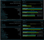
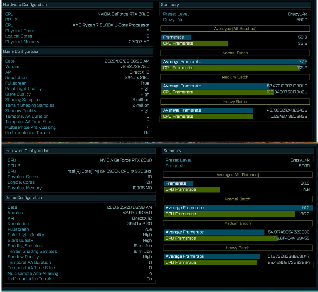
Today, we have gotten the first benchmark of AMD's upcoming Ryzen 7 5800X CPU. Thanks to the popular hardware leaker, TUP APISAK, we have the first benchmark of the new Vermeer processor, compared to Intel's latest and greatest - Core i9-10900K. The AMD processor is an eight-core, sixteen threaded model compared to the 10C/20T Intel processor. While we do not know the final clocks of the AMD CPU, we could assume that the engineering sample was used and we could see an even higher performance. Below you can see the performance of the CPU and how it compares to Intel. By the numbers shown, we can expect AMD to possibly be a new gaming king, as the numbers are very close to Intel. The average batch result for the Ryzen 7 5800X was 59.3 FPS and when it comes to CPU frames it managed to score 133.6 FPS. Intel's best managed to average 60.3 FPS and 114.8 FPS from the CPU framerates. Both systems were tested with NVIDIA's GeForce RTX 2080 GPUs.
Source:
@TUM_APISAK (Twitter)
Today, we have gotten the first benchmark of AMD's upcoming Ryzen 7 5800X CPU. Thanks to the popular hardware leaker, TUP APISAK, we have the first benchmark of the new Vermeer processor, compared to Intel's latest and greatest - Core i9-10900K. The AMD processor is an eight-core, sixteen threaded model compared to the 10C/20T Intel processor. While we do not know the final clocks of the AMD CPU, we could assume that the engineering sample was used and we could see an even higher performance. Below you can see the performance of the CPU and how it compares to Intel. By the numbers shown, we can expect AMD to possibly be a new gaming king, as the numbers are very close to Intel. The average batch result for the Ryzen 7 5800X was 59.3 FPS and when it comes to CPU frames it managed to score 133.6 FPS. Intel's best managed to average 60.3 FPS and 114.8 FPS from the CPU framerates. Both systems were tested with NVIDIA's GeForce RTX 2080 GPUs.
82 Comments on First Signs of AMD Zen 3 "Vermeer" CPUs Surface, Ryzen 7 5800X Tested
The differences are probably in what a "typical workload" is. Intel is not slower in all non-gaming workloads, that's a false narrative.
As example, look under the 10900K review on this site under "Science and Research" and you'll find it is a clean sweep win for Intel. Look under "Office and Productivity" and it's the same clean sweep for Intel. Web Browsing, Development, and server/workstation are a mixed bag between Intel and AMD. Only under Rendering and Compression/Encryption does AMD take a clear win. If rendering and compression/encryption is your main form of productivity AMD is your clear choice, but I would say that does not describe how the majority of people use their PCs.
www.techpowerup.com/review/intel-core-i9-10850k/9.html
Its no longer a matter of "speeding up instructions", but instead a matter of "keeping the pipelines full, so that as many instructions can be executed in parallel as possible". Its been like this since 1995 when the Pentium Pro introduced out-of-order execution to the consumer (and several other computers had OoO execution in the decades before Pentium Pro)
You already have Threadripper and Epyc with more memory bandwidth, and you can see it only helps select workloads which are very data intensive, not single threaded performance in general, which is mostly limited by memory latency and pipeline flushes.To the extent that I can understand what you're saying, caches are already sort of doing this. Caches are divided into banks, and the CPU cycles through them to read/write, in order to maximize bandwidth. Memory work in a very similar way.Cache misses occur because something is not in cache, and it stalls the thread until the required data is retrieved. CPUs currently use SMT to "work around" this, by executing something else during idle cycles, but it doesn't help single threaded performance. I don't understand how modulating caches could help either, so please elaborate.
Some of the things which could help though; (on the hardware side)
- Larger caches - for things that are pushed out, but not things that are unpredictable.
- Larger instruction window (OoO window) - hide some latency by executing some things earlier, but it can't solve everything.
- Reducing cache latency
- Redesigning the cache hierarchy
- Increasing the CPU's ability to execute some things during stalls - making them more partial stalls, beyond just increasing the OoO window. I'm curious to see what the research into "threadlets" will lead to.
See appendix D:
software.intel.com/content/www/us/en/develop/download/intel-64-and-ia-32-architectures-optimization-reference-manual.html
IMUL: 1x per clock. ADD/SUB is 3x to 4x per clock cycle. LEA is 2x per clock cycle throughput.
Look at the instructions that take a long time: none of them are expected to be used in the inner loop. "lock cmpxchg" is an inter-thread synchronization instruction, likely to be limited by L3 cache or DDR4 RAM. CPUID is never going to be called in the inner-loop. CLFLUSH (cacheline flush) is also a memory-ordering / inter-thread synchronization thing, and I don't expect it to be in anyone's innerloop.
The only instruction that may need improvement is DIV / IDIV. I'll talk about that later.
---------
Lets check the 256-bit AVX instructions?
Oh wow, virtually everything on this page is throughput of 0.33, 0.5, or 1. (3x per clock, 2x per clock, and 1x per clock cycle). This includes the ever important 256-bit VPMADD instruction (vectorized multiply-and-add instruction), with a throughput of either 2x per clock (0.5), or 1x per clock.
For every single performance-critical instruction, the pattern continues. Intel, AMD, and ARM have optimized these instructions to an incredible, and ridiculous degree.
----------
IDIV and DIV are maybe your only exception, which handle not only division but also modulo (%) operations. But it seems like most performance critical code avoids division and favors either inverse-multiplication (with the inverse figured out by the compiler), the use of bitshifts, or in some rare cases, the use of floating-point division (which is much faster).
godbolt.org/z/zWaWjh
See how "divide by 31" becomes an imul instruction by most compilers (multiplication of the integer-multiplication inverse), avoiding the use of division. I'm constantly surprised at how good compilers are at removing spurious divisions or modulo operations from my code (and a good old subtract loop handles most "dynamic division" cases in my experience)
I guess it saw this news article. :p