Monday, April 11th 2022

NVIDIA Claims Grace CPU Superchip is 2X Faster Than Intel Ice Lake
When NVIDIA announced its Grace CPU Superchip, the company officially showed its efforts of creating an HPC-oriented processor to compete with Intel and AMD. The Grace CPU Superchip combines two Grace CPU modules that use the NVLink-C2C technology to deliver 144 Arm v9 cores and 1 TB/s of memory bandwidth. Each core is Arm Neoverse N2 Perseus design, configured to achieve the highest throughput and bandwidth. As far as performance is concerned, the only detail NVIDIA provides on its website is the estimated SPECrate 2017_int_base score of over 740. Thanks to the colleges over at Tom's Hardware, we have another performance figure to look at.
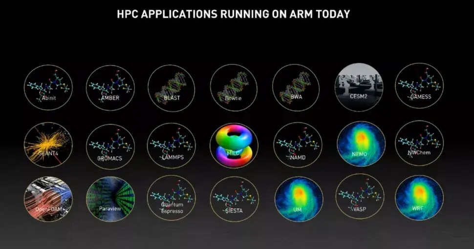
NVIDIA has made a slide about comparison with Intel's Ice Lake server processors. One Grace CPU Superchip was compared to two Xeon Platinum 8360Y Ice Lake CPUs configured in a dual-socket server node. The Grace CPU Superchip outperformed the Ice Lake configuration by two times and provided 2.3 times the efficiency in WRF simulation. This HPC application is CPU-bound, allowing the new Grace CPU to show off. This is all thanks to the Arm v9 Neoverse N2 cores pairing efficiently with outstanding performance. NVIDIA made a graph showcasing all HPC applications running on Arm today, with many more to come, which you can see below. Remember that NVIDIA provides this information, so we have to wait for the 2023 launch to see it in action.


Source:
Tom's Hardware
NVIDIA has made a slide about comparison with Intel's Ice Lake server processors. One Grace CPU Superchip was compared to two Xeon Platinum 8360Y Ice Lake CPUs configured in a dual-socket server node. The Grace CPU Superchip outperformed the Ice Lake configuration by two times and provided 2.3 times the efficiency in WRF simulation. This HPC application is CPU-bound, allowing the new Grace CPU to show off. This is all thanks to the Arm v9 Neoverse N2 cores pairing efficiently with outstanding performance. NVIDIA made a graph showcasing all HPC applications running on Arm today, with many more to come, which you can see below. Remember that NVIDIA provides this information, so we have to wait for the 2023 launch to see it in action.


30 Comments on NVIDIA Claims Grace CPU Superchip is 2X Faster Than Intel Ice Lake
Intel also has a singular "aesenc" function, while ARM has to do "aese + aesmc" (aes-encrypt plus aes-mix-columns, because ARM split this up into two different instructions). Things get ridiculous when we get into ARM-NEON instructions. There's literally 450 ways to load or store a SIMD register in ARM-NEON.
I'm not kidding: developer.arm.com/architectures/instruction-sets/intrinsics/#f:@navigationhierarchiessimdisa=[Neon]&f:@navigationhierarchiesinstructiongroup=[Load,Stride]
"Reduced" my ass. The reason this exists is because ARM has a bunch of hardcoded ways to read/write to memory to coincide with the stupid number of file-formats (especially video formats) that exist out there. By hard-coding an ASIC to read/write memory in the right order, ARM reduces the amount of power per load operation, making video processing (aka: Youtube) ever so slightly more power-efficient.
EDIT: If you're interested in the details: community.arm.com/arm-community-blogs/b/architectures-and-processors-blog/posts/coding-for-neon---part-1-load-and-stores
If you want high-speed and low-power usage per instruction, you make extremely specific instructions, such as vector-load interleave-pattern 2 16-bit. (Aka: the vld 2 . 16 instruction). You know, not to be confused with vld 4 .8 or vld 1 .32. These instructions exist because video codecs are in YUV444 vs YUV420 or RGB888, or RGBA8888 formats, and video reading / multimedia programs have to decode them and handle all of the possibilities efficiently.
I've said it before and I'll say it again: ARM is CISC these days. Its kind of ridiculous how specific their instructions get, in this case more specific than Intel (who just implemented the "pshufb" instruction instead). GPUs probably have the most elegant solution: "shared" memory that acts as a crossbar that can implement arbitrary shuffles as needed (instead of needing hundreds of instructions to handle every combination of 128-bit 1/2/4-way interleaved 8/16/32 bit patterns)
And I mean VERY, IE full of shite.