Wednesday, June 26th 2024

Intel Demonstrates First Fully Integrated Optical IO Chiplet
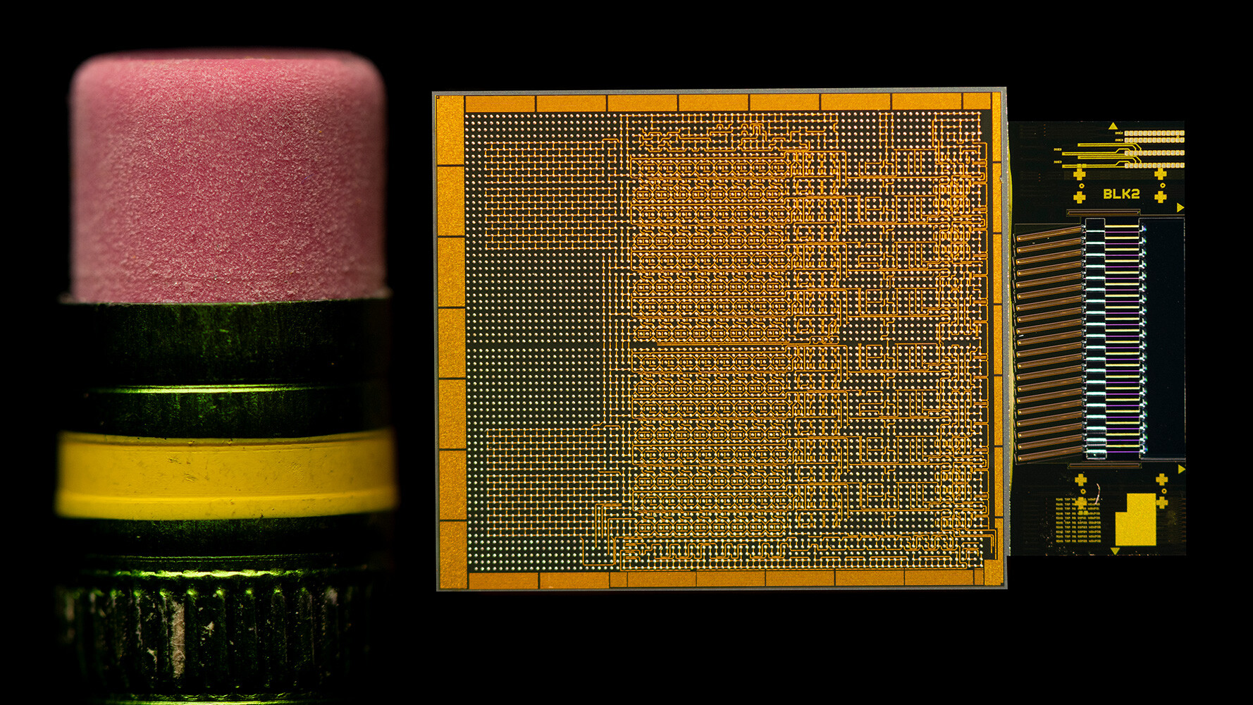
Intel Corporation has achieved a revolutionary milestone in integrated photonics technology for high-speed data transmission. At the Optical Fiber Communication Conference (OFC) 2024, Intel's Integrated Photonics Solutions (IPS) Group demonstrated the industry's most advanced and first-ever fully integrated optical compute interconnect (OCI) chiplet co-packaged with an Intel CPU and running live data. Intel's OCI chiplet represents a leap forward in high-bandwidth interconnect by enabling co-packaged optical input/output (I/O) in emerging AI infrastructure for data centers and high performance computing (HPC) applications.
"The ever-increasing movement of data from server to server is straining the capabilities of today's data center infrastructure, and current solutions are rapidly approaching the practical limits of electrical I/O performance. However, Intel's groundbreaking achievement empowers customers to seamlessly integrate co-packaged silicon photonics interconnect solutions into next-generation compute systems. Our OCI chiplet boosts bandwidth, reduces power consumption and increases reach, enabling ML workload acceleration that promises to revolutionize high-performance AI infrastructure," said Thomas Liljeberg, senior director, Product Management and Strategy, Integrated Photonics Solutions (IPS) Group.
 This first OCI chiplet is designed to support 64 channels of 32 gigabits per second (Gbps) data transmission in each direction on up to 100 meters of fiber optics and is expected to address AI infrastructure's growing demands for higher bandwidth, lower power consumption and longer reach. It enables future scalability of CPU/GPU cluster connectivity and novel compute architectures, including coherent memory expansion and resource disaggregation.
AI-based applications are increasingly deployed globally, and recent developments in large language models (LLM) and generative AI are accelerating that trend. Larger and more efficient machine learning (ML) models will play a key role in addressing the emerging requirements of AI acceleration workloads. The need to scale future computing platforms for AI is driving exponential growth in I/O bandwidth and longer reach to support larger processing unit (CPU/GPU/IPU) clusters and architectures with more efficient resource utilization, such as xPU disaggregation and memory pooling.
Electrical I/O (i.e., copper trace connectivity) supports high bandwidth density and low power, but only offers short reaches of about one meter or less. Pluggable optical transceiver modules used in data centers and early AI clusters can increase reach at cost and power levels that are not sustainable with the scaling requirements of AI workloads. A co-packaged xPU optical I/O solution can support higher bandwidths with improved power efficiency, low latency and longer reach - exactly what AI/ML infrastructure scaling requires.
As an analogy, replacing electrical I/O with optical I/O in CPUs and GPUs to transfer data is like going from using horse carriages to distribute goods, limited in capacity and range, to using cars and trucks that can deliver much larger quantities of goods over much longer distances. This level of improved performance and energy cost is what optical I/O solutions like Intel's OCI chiplet emerging bring to AI scaling.
The fully Integrated OCI chiplet leverages Intel's field-proven silicon photonics technology and integrates a silicon photonics integrated circuit (PIC), which includes on-chip lasers and optical amplifiers, with an electrical IC. The OCI chiplet demonstrated at OFC was co-packaged with an Intel CPU but can also be integrated with next-generation CPUs, GPUs, IPUs and other system-on-chips (SoCs).
This first OCI implementation supports up to 4 terabits per second (Tbps) bidirectional data transfer, compatible with peripheral component interconnect express (PCIe) Gen5. The live optical link demonstration showcases a transmitter (Tx) and receiver (Rx) connection between two CPU platforms over a single-mode fiber (SMF) patch cord. The CPUs generated and measured the optical Bit Error Rate (BER), and the demo showcases the Tx optical spectrum with 8 wavelengths at 200 gigahertz (GHz) spacing on a single fiber, along with a 32 Gbps Tx eye diagram illustrating strong signal quality.
The current chiplet supports 64 channels of 32 Gbps data in each direction up to 100 meters (though practical applications may be limited to tens of meters due to time-of-flight latency), utilizing eight fiber pairs, each carrying eight dense wavelength division multiplexing (DWDM) wavelengths. The co-packaged solution is also remarkably energy efficient, consuming only 5 pico-Joules (pJ) per bit compared to pluggable optical transceiver modules at about 15 pJ/bit. This level of hyperefficiency is critical for data centers and high-performance computing environments and could help address AI's unsustainable power requirements.
As a market leader in silicon photonics, Intel leverages more than 25 years of internal research from Intel Labs, which pioneered integrated photonics. Intel was the first company to develop and ship silicon photonics-based connectivity products with industry-leading reliability at high volume to major cloud service providers.
Intel's main differentiator is unparalleled integration using hybrid laser-on-wafer technology and direct integration, which yield higher reliability and lower costs. This unique approach enables Intel to deliver superior performance while maintaining efficiency. Intel's robust, high-volume platform boasts shipping over 8 million PICs with over 32 million integrated on-chip lasers, showing a laser failures-in-time (FIT) rate of less than 0.1, a widely utilized measure of reliability that represents failure rates and how many failures occur.
These PICs were packaged in pluggable transceiver modules, deployed in large data center networks at major hyperscale cloud service providers for 100, 200, and 400 Gbps applications. Next generation, 200G/lane PICs to support emerging 800 Gbps and 1.6 Tbps applications are under development.
Intel is also implementing a new silicon photonics fab process node with state-of-the-art (SOA) device performance, higher density, better coupling and vastly improved economics. Intel continues to make advancements in on-chip laser and SOA performance, cost (greater than 40% die area reduction) and power (greater than 15% reduction).
Intel's current OCI chiplet is a prototype. Intel is working with select customers to co-package OCI with their SOCs as an optical I/O solution.
Intel's OCI chiplet represents a leap forward in high-speed data transmission. As the AI infrastructure landscape evolves, Intel remains at the forefront, driving innovation and shaping the future of connectivity.
"The ever-increasing movement of data from server to server is straining the capabilities of today's data center infrastructure, and current solutions are rapidly approaching the practical limits of electrical I/O performance. However, Intel's groundbreaking achievement empowers customers to seamlessly integrate co-packaged silicon photonics interconnect solutions into next-generation compute systems. Our OCI chiplet boosts bandwidth, reduces power consumption and increases reach, enabling ML workload acceleration that promises to revolutionize high-performance AI infrastructure," said Thomas Liljeberg, senior director, Product Management and Strategy, Integrated Photonics Solutions (IPS) Group.

AI-based applications are increasingly deployed globally, and recent developments in large language models (LLM) and generative AI are accelerating that trend. Larger and more efficient machine learning (ML) models will play a key role in addressing the emerging requirements of AI acceleration workloads. The need to scale future computing platforms for AI is driving exponential growth in I/O bandwidth and longer reach to support larger processing unit (CPU/GPU/IPU) clusters and architectures with more efficient resource utilization, such as xPU disaggregation and memory pooling.
Electrical I/O (i.e., copper trace connectivity) supports high bandwidth density and low power, but only offers short reaches of about one meter or less. Pluggable optical transceiver modules used in data centers and early AI clusters can increase reach at cost and power levels that are not sustainable with the scaling requirements of AI workloads. A co-packaged xPU optical I/O solution can support higher bandwidths with improved power efficiency, low latency and longer reach - exactly what AI/ML infrastructure scaling requires.
As an analogy, replacing electrical I/O with optical I/O in CPUs and GPUs to transfer data is like going from using horse carriages to distribute goods, limited in capacity and range, to using cars and trucks that can deliver much larger quantities of goods over much longer distances. This level of improved performance and energy cost is what optical I/O solutions like Intel's OCI chiplet emerging bring to AI scaling.
The fully Integrated OCI chiplet leverages Intel's field-proven silicon photonics technology and integrates a silicon photonics integrated circuit (PIC), which includes on-chip lasers and optical amplifiers, with an electrical IC. The OCI chiplet demonstrated at OFC was co-packaged with an Intel CPU but can also be integrated with next-generation CPUs, GPUs, IPUs and other system-on-chips (SoCs).
This first OCI implementation supports up to 4 terabits per second (Tbps) bidirectional data transfer, compatible with peripheral component interconnect express (PCIe) Gen5. The live optical link demonstration showcases a transmitter (Tx) and receiver (Rx) connection between two CPU platforms over a single-mode fiber (SMF) patch cord. The CPUs generated and measured the optical Bit Error Rate (BER), and the demo showcases the Tx optical spectrum with 8 wavelengths at 200 gigahertz (GHz) spacing on a single fiber, along with a 32 Gbps Tx eye diagram illustrating strong signal quality.
The current chiplet supports 64 channels of 32 Gbps data in each direction up to 100 meters (though practical applications may be limited to tens of meters due to time-of-flight latency), utilizing eight fiber pairs, each carrying eight dense wavelength division multiplexing (DWDM) wavelengths. The co-packaged solution is also remarkably energy efficient, consuming only 5 pico-Joules (pJ) per bit compared to pluggable optical transceiver modules at about 15 pJ/bit. This level of hyperefficiency is critical for data centers and high-performance computing environments and could help address AI's unsustainable power requirements.
As a market leader in silicon photonics, Intel leverages more than 25 years of internal research from Intel Labs, which pioneered integrated photonics. Intel was the first company to develop and ship silicon photonics-based connectivity products with industry-leading reliability at high volume to major cloud service providers.
Intel's main differentiator is unparalleled integration using hybrid laser-on-wafer technology and direct integration, which yield higher reliability and lower costs. This unique approach enables Intel to deliver superior performance while maintaining efficiency. Intel's robust, high-volume platform boasts shipping over 8 million PICs with over 32 million integrated on-chip lasers, showing a laser failures-in-time (FIT) rate of less than 0.1, a widely utilized measure of reliability that represents failure rates and how many failures occur.
These PICs were packaged in pluggable transceiver modules, deployed in large data center networks at major hyperscale cloud service providers for 100, 200, and 400 Gbps applications. Next generation, 200G/lane PICs to support emerging 800 Gbps and 1.6 Tbps applications are under development.
Intel is also implementing a new silicon photonics fab process node with state-of-the-art (SOA) device performance, higher density, better coupling and vastly improved economics. Intel continues to make advancements in on-chip laser and SOA performance, cost (greater than 40% die area reduction) and power (greater than 15% reduction).
Intel's current OCI chiplet is a prototype. Intel is working with select customers to co-package OCI with their SOCs as an optical I/O solution.
Intel's OCI chiplet represents a leap forward in high-speed data transmission. As the AI infrastructure landscape evolves, Intel remains at the forefront, driving innovation and shaping the future of connectivity.
11 Comments on Intel Demonstrates First Fully Integrated Optical IO Chiplet
Doubt it would be seen in consumer hardware for another couple decades, if ever. But one can dream.