News Posts matching #Zen 4

Return to Keyword Browsing

AMD Said to Become TSMC's Third Largest Customer in 2023

Based on a report in the Taiwanese media, AMD is quickly becoming a key customer for TSMC and is expected to become its third largest customer in 2023. This is partially due to new orders that AMD has placed with TSMC for its 5 nm node. AMD is said to become TSMC's single largest customer for its 5 nm node in 2023, although it's not clear from the report how large of a share of the 5 nm node AMD will have.

The additional orders are said to be related to AMD's Zen 4 based processors, as well as its upcoming RDNA3 based GPUs. AMD is expected to be reaching a production volume of some 20,000 wafers in the fourth quarter of 2022, although there's no mention of what's expected in 2023. Considering most of AMD's products for the next year or two will all be based on TSMC's 5 nm node, this shouldn't come as a huge surprise though, as AMD has a wide range of new CPU and GPU products coming.

AMD's Second Socket AM5 Ryzen Processor will be "Granite Ridge," Company Announces "Phoenix Point"

AMD in its 2022 Financial Analyst Day presentation announced the codename for the second generation of Ryzen desktop processors for Socket AM5, which is "Granite Ridge." A successor to the Ryzen 7000 "Raphael," the next-generation "Granite Ridge" processor will incorporate the "Zen 5" CPU microarchitecture, with its CPU complex dies (CCDs) built on the 4 nm silicon fabrication node. "Zen 5" will feature several core-level designs as detailed in our older article, including a redesigned front-end with greater parallelism, which should indicate a much large execution stage. The architecture could also incorporate AI/ML performance enhancements as AMD taps into Xilinx IP to add more fixed-function hardware backing the AI/ML capabilities of its processors.

The "Zen 5" microarchitecture makes its client debut with Ryzen "Granite Ridge," and server debut with EPYC "Turin." It's being speculated that AMD could give "Turin" a round of CPU core-count increases, while retaining the same SP5 infrastructure; which means we could see either smaller CCDs, or higher core-count per CCD with "Zen 5." Much like "Raphael," the next-gen "Granite Ridge" will be a series of high core-count desktop processors that will feature a functional iGPU that's good enough for desktop/productivity, though not gaming. AMD confirmed that it doesn't see "Raphael" as an APU, and that its definition of an "APU" is a processor with a large iGPU that's capable of gaming. The company's next such APU will be "Phoenix Point."

AMD Makes 3DV Cache a Part of its Long-term Roadmap, Announces Genoa-X and Siena

AMD in its recent interview with TechPowerUp had asserted that 3D Vertical Cache (or 3DV Cache), isn't a one-off technology and that it would be a continual part of its roadmap. In its 2022 Financial Analyst Day presentation, the company confirmed this, by announcing variants of its CPU chiplets that have 3DV Cache, extending to both the upcoming "Zen 4" microarchitecture, and the upcoming "Zen 5," which it unveiled today.

EPYC "Genoa" is codename for the upcoming line of server processors based on the "Zen 4" CPU microarchitecture, with CPU core-counts of up to 96-core/192-thread. These feature the standard "Zen 4" CCD. The company hasn't yet announced the last-level cache (L3 cache) size of the standard "Zen 4" CCD. The company will launch the EPYC "Genoa-X" processor, which much like the EPYC "Milan-X," will incorporate 3DV Cache, with a stacked L3 cache die on top of the chiplet. "Genoa-X" is slated for a 2023 debut.

AMD's Upcoming Zen 4 CPU Delidded by Overclocker

It appears that AMD's Zen 4 based CPUs are making their ways into the hands of overclockers and so far at least one has already been delidded. Although we only get to see the IHS itself, it's clearly very thick compared to what we've seen in the past, although it appears to be fairly straightforward to remove, if it wasn't for the fact that the two CCD's and the IOD are soldered to it. Unlike current CPUs, which have a solid seal, the Zen 4 CPUs appear to only have the IHS glued to the CPU packaging in a few spots.

Judging by the looks of the area where the CCDs and the IOD attach to the IHS, this looks like a destructive delidding, although it could just be leftovers from the soldering material. The IHS has clearly been coated with some materials for a good solder interface as well, but this is nothing new, as we've seen this on delidded, soldered CPUs in the past. The person who shared this picture should most likely not have done so and as such, we won't be posting a link to the source.

DDR5 Memory Pricing Declining, Bolstering Hope for Next-Gen Platform Costs

DDR5 memory pricing has been declining faster than expected, with average pricing for modules based on the latest standard dropping by as much as 20% in a month's time. As reported by ComputerBase, pricing for 1 GB of DDR5 has fallen from around €15 by the end of 2021 down to around €5/GB at time of writing. At current pricing, an entry-level, 32 GB DDR5 kit DDR5-4800 memory (JEDEC standard) has fallen from a high of €430 down to a much more palatable €154.

The price decline comes as good news for anyone aiming to upgrade their PC in wake of AMD's Socket AM5 launch for its Zen 4 architecture, which the company has already confirmed will only support the latest RAM standard. AMD itself must be riding the sea of relief, as high DDR5 pricing could significantly shape the company's next-gen platform's value compared to arch-rival Intel, which already offers DDR4 and DDR5 support with its Alder Lake chips. Expectations place the same memory support for the next-gen Raptor Lake platform. Prices for DDR4 memory seem to have hit a bottom, however, as pricing hasn't significantly moved in around six months. Like with all new technologies, expect the price difference to eventually change in favor of DDR5 memory, as manufacturers adjust their outputs towards adoption.

AMD Clarifies Ryzen 7000 "Zen 4" TDP and Power Limits: 170W TDP, 230W PPT

The mention of "170 W" in one of the slides of AMD's Computex 2022 reveal of the upcoming Ryzen 7000 "Zen 4" desktop processors, caused quite some confusion as to what that figure meant. AMD issued a structured clarification on the matter, laying to rest the terminology associated with it. Apparently, there will be certain SKUs of Socket AM5 processors with TDP of 170 W. This would be the same classical definition of TDP that AMD has been consistently using. The package-power tracking (PPT), a figure that translates as power limit for the socket, is 230 W.

This does not necessarily mean that there will be a Ryzen 7000-series SKU with 170 W TDP. AMD plans to give AM5 a similar life-cycle to AM4, which is now spanning five generations of Ryzen processors, and the 170 W TDP and 230 W PPT figures only denote design goals for the socket. AMD, in a statement, explained why it needed to make AM5 capable of delivering much higher power than AM4 could—to enable higher CPU core-counts in the future, more on-package hardware, and for new capabilities like power-hungry instruction-sets (think AVX-512). AMD has been calculating PPT as 1.35 times TDP, since the very first generation of Ryzen chips. For a 105 W TDP processor, this means 140 W PPT, and the same formula continues with Ryzen 7000 series (230 W is 1.35x 170 W).
The AMD statement follows.

Team Group's DDR5 Industrial Server Memory Officially in Mass Production

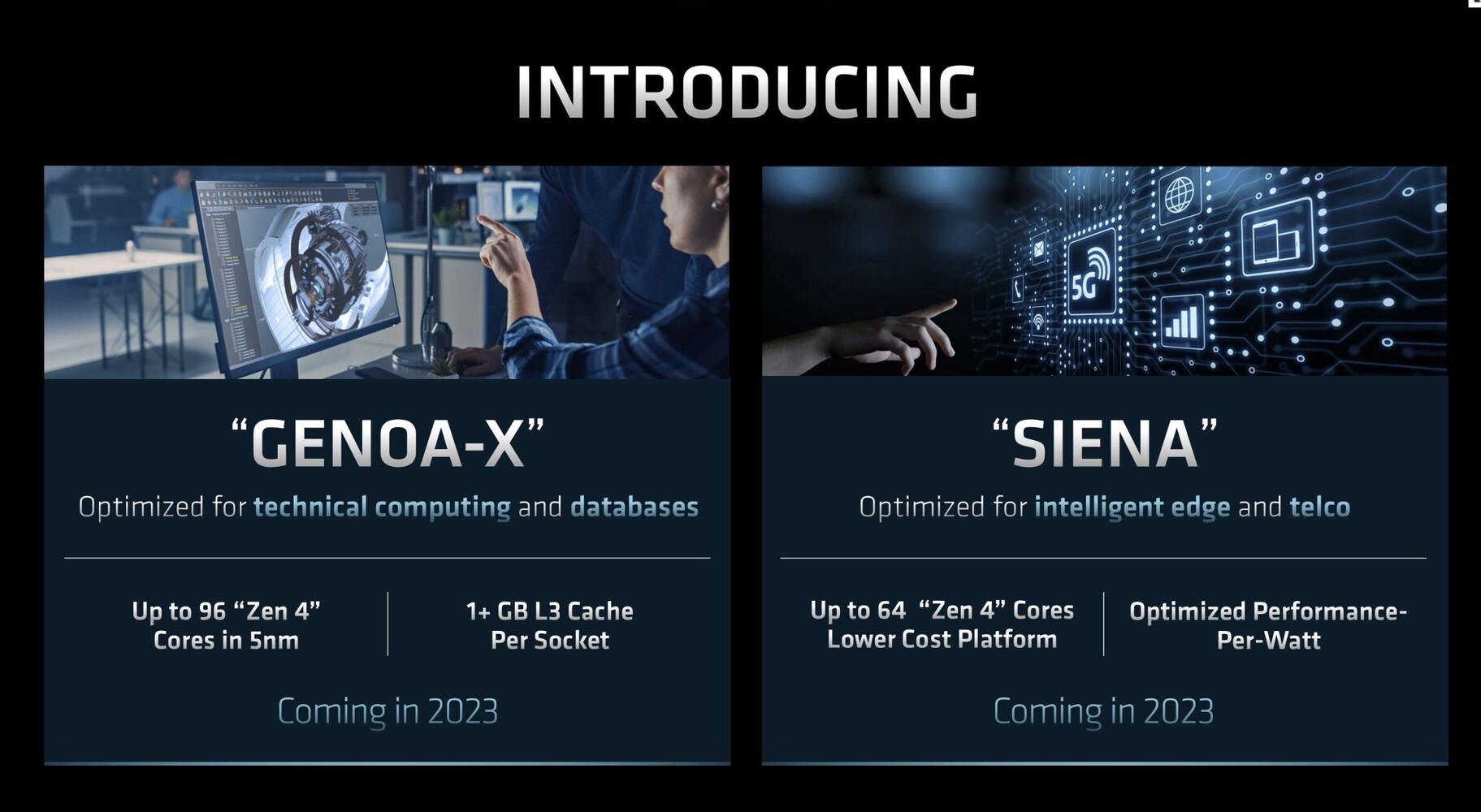
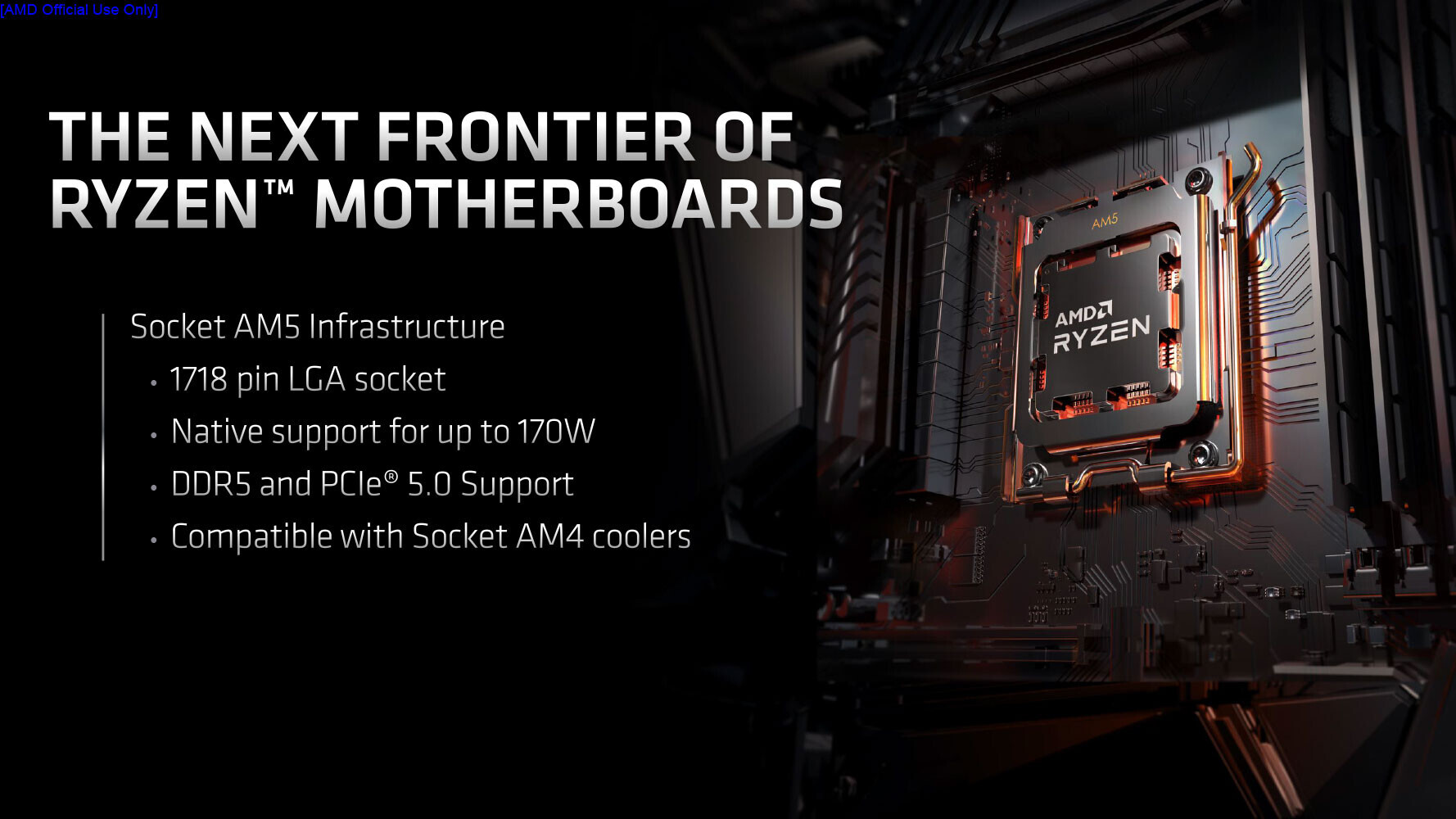
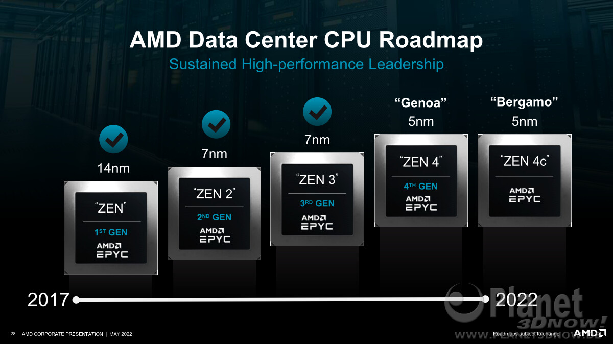
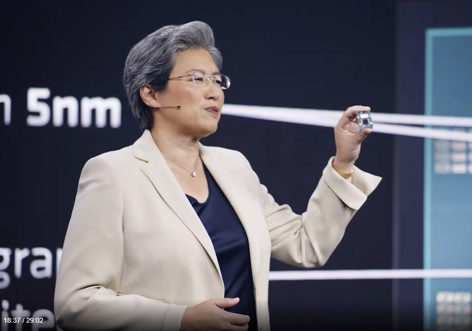
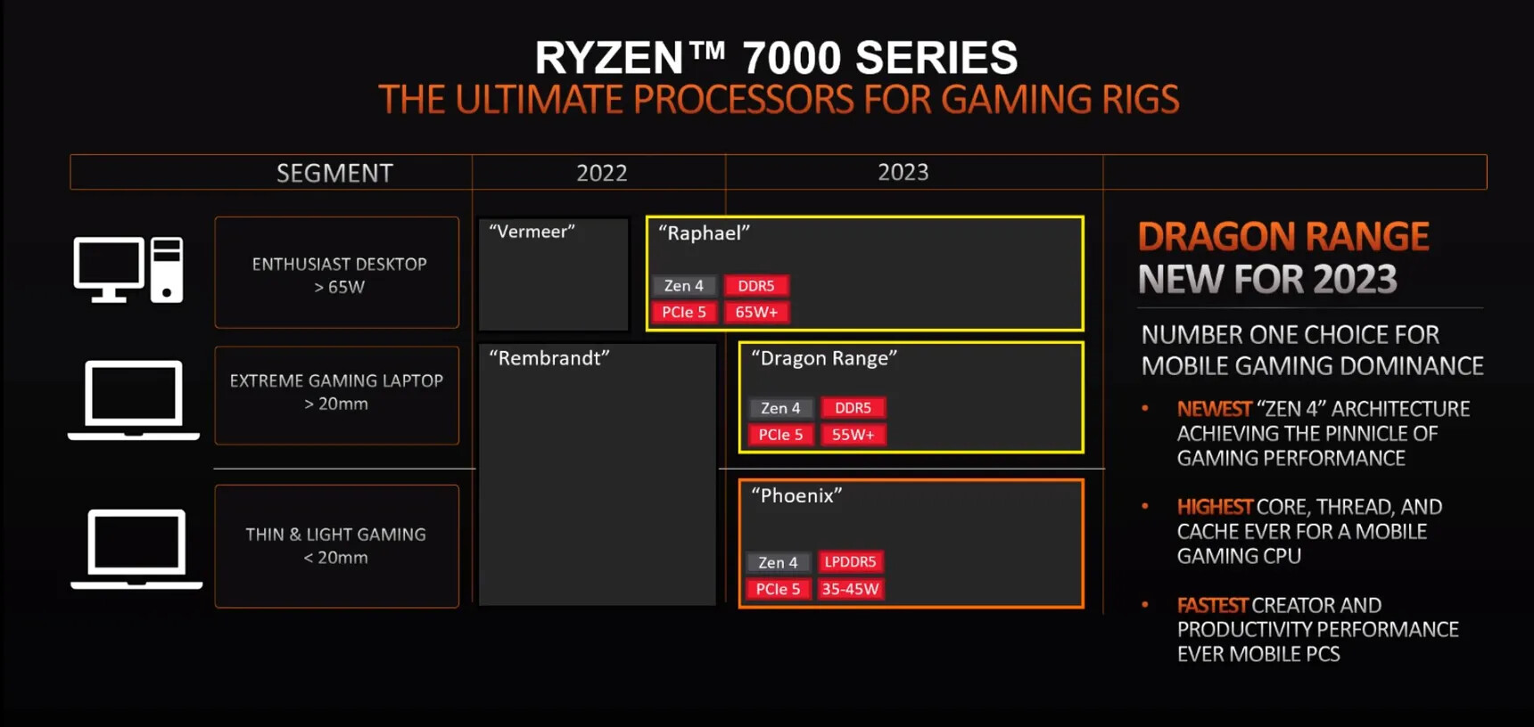
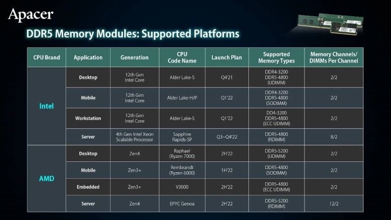
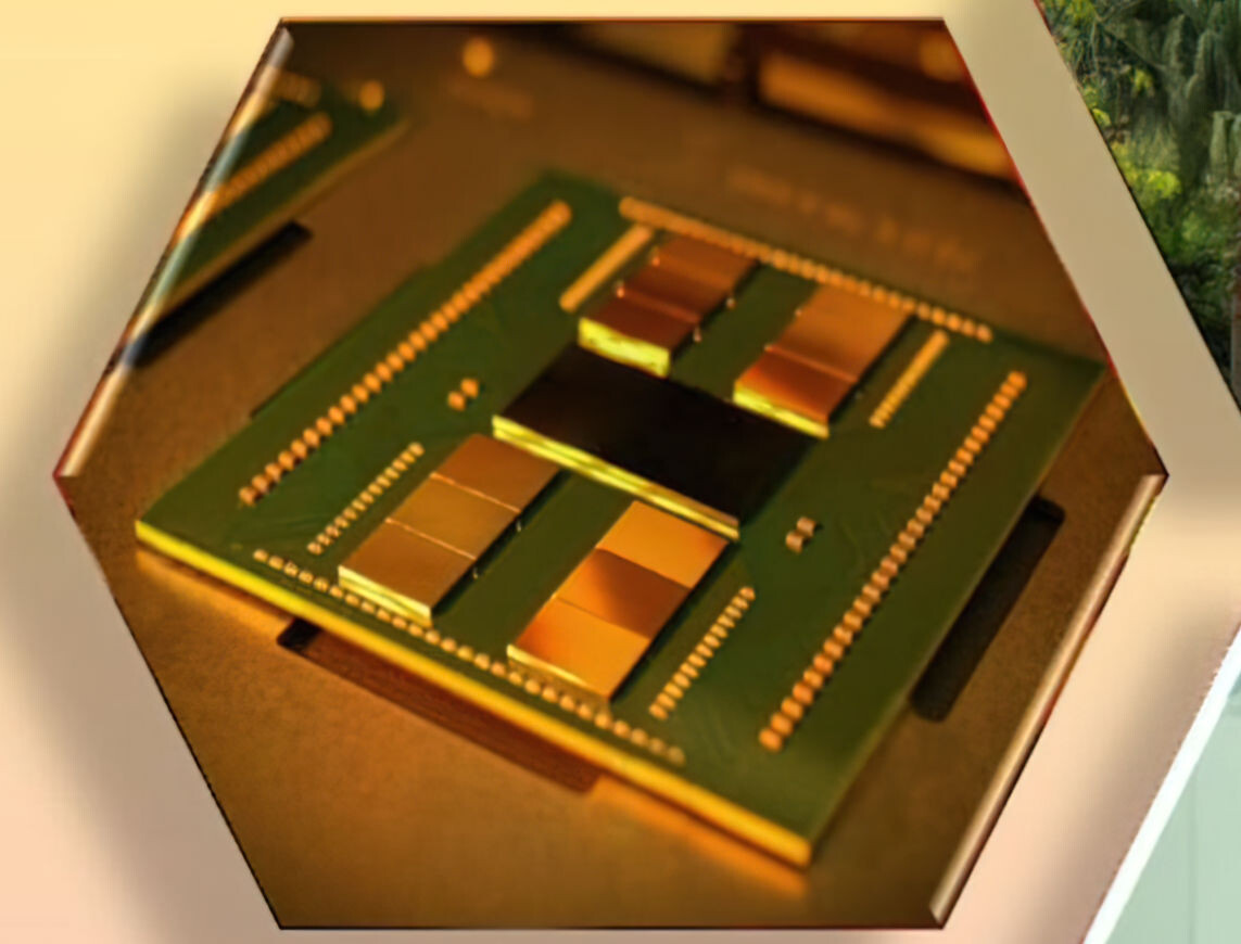
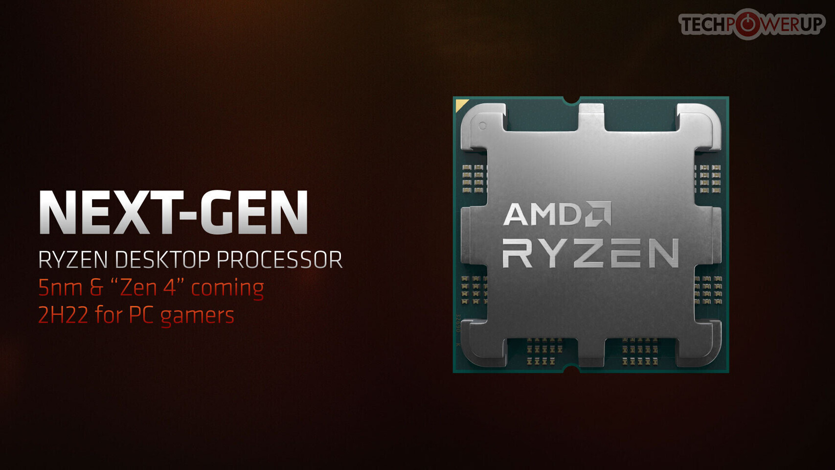
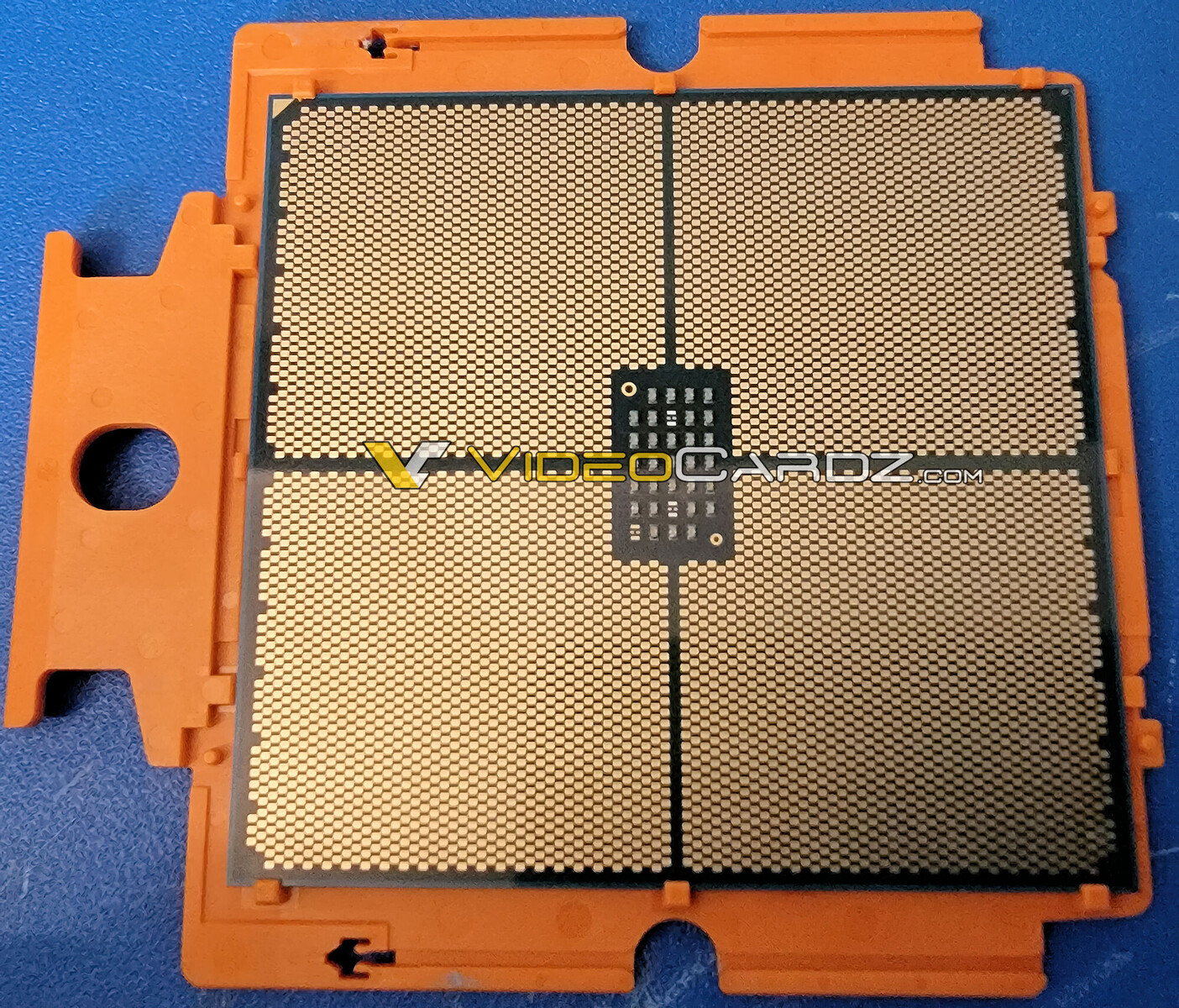
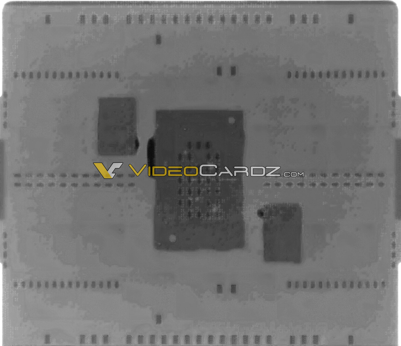
To usher in the new era of DDR5 and satisfy the demands for precise, high-performance, real-time computing, and computer multi-tasking in servers, data centers, and industrial computers, the world-leading memory brand TEAMGROUP is officially announcing today that TEAMGROUP's DDR5 Industrial Server Memory is now in mass production. The DDR5 Industrial Server Memory targets applications in high-end servers and large databases and is integrated with TEAMGROUP's patented technology, welcoming a total upgrade for next-generational servers such as Intel Eagle Stream and AMD Zen 4 Genoa.

TEAMGROUP's DDR5 ECC DIMM and DDR5 R-DIMM Industrial Server Memory modules can reach speeds of up to 6400MT/s and storage capacities of up to 128 GB, with total energy consumption reduced to 1.1 V. TEAMGROUP has also introduced Row Hammer Protection Technology to support the DFE (Decision Feedback Equalization) function to offer robust support for data storage. The memory is equipped with TEAMGROUP's patented "TRUST technology", which stands for Temperature, Robust, Unique, S.M.A.R.T. technology, and Trusty. With the TRUST technology, the industrial server memory can ensure reliable performance under harsh environments of high temperatures, high humidity, sulfurization, vibration, and shock as well as improving the overall reliability and durability of the product to guarantee that the memory can satisfy the diversified demands of next-gen servers. In addition, the DDR5 Industrial Server Memory has adopted a brand new framework. The greatest difference between the DDR5 and DDR4 server memories is that the power management is now transferred onto the DIMM, in other words, TEAMGROUP has optimized redundant circuit designs on the server, providing its DDR5 products a greater system stability, lower power consumption, better performances, larger capacities, and more stable signals.

AMD EPYC "Bergamo" 128-core Processor Based on Same SP5 Socket as "Genoa"

AMD is launching two distinct classes of next-generation enterprise processors, the 4th Generation EPYC "Genoa" with CPU core-counts up to 96-core/192-thread; and the new EPYC "Bergamo" with a massive 128-core/256-thread compute density. Pictures of the "Genoa" MCM are already out in the wild, revealing twelve "Zen 4" CCDs built on 5 nm, and a new-generation sIOD (I/O die) that's very likely built on 6 nm. The fiberglass substrate of "Genoa" already looks crowded with twelve chiplets, making us wonder if AMD needed a larger package for "Bergamo." Turns out, it doesn't.

In its latest Corporate presentation, AMD reiterated that "Bergamo" will be based on the same SP5 (LGA-6096) package as "Genoa." This would mean that the company either made room for more CCDs, or the CCDs themselves are larger in size. AMD states that "Bergamo" CCDs are based on the "Zen 4c" microarchitecture. Details about "Zen 4c" are scarce, but from what we gather, it is a cloud-optimized variant of "Zen 4" probably with the entire ISA of "Zen 4," and power characteristics suited for high-density cloud environments. These chiplets are built on the same TSMC N5 (5 nm EUV) process as the regular "Zen 4" CCDs.

Hands On with the new Gigabyte X670 Motherboards at Computex 2022

Computex 2022 is what's being referred to as a hybrid show and although most of the motherboard manufacturers chose not to exhibit this year, Gigabyte was at the show and we got to take a closer look at its new AM5 motherboards. Gigabyte was only showing four models, but on the plus side, the staff at the booth was more than happy to share details about the boards with us. The four boards on display were the X670E Aorus Xtreme, the X670E Aorus Master, the X670E Aero D and the X670 Aorus Pro AX. Note that these were early board revision and the E is missing in the model name from three of the models, which suggests that AMD hadn't informed the board makers about this distinction between its chipsets until earlier this month when rumours about it started to appear online.

Gigabyte will have a full lineup of boards coming later this year when AMD launches its AM5 platform, although based on the information we were given, the majority of its boards will be based on the B650 chipset. We should point out that there will be high-end B650 motherboards that will be priced similar to lower-end X670 models, which means that buying AM5 motherboards will be highly dependent on what features you favour. Unfortunately no B650 motherboards were on display and we won't be sharing any details of these models at this time. As for the X670E versus X670 chipsets, as there are of course two per board, it seems like the difference comes down to PCIe 5.0 or PCIe 4.0 for the x16 PCIe slot as the major differentiator between Gigabyte's different SKUs.

AMD Unveils 5 nm Ryzen 7000 "Zen 4" Desktop Processors & AM5 DDR5 Platform

AMD today unveiled its next-generation Ryzen 7000 desktop processors, based on the Socket AM5 desktop platform. The new Ryzen 7000 series processors introduce the new "Zen 4" microarchitecture, with the company claiming a 15% single-threaded uplift over "Zen 3" (16-core/32-thread Zen 4 processor prototype compared to a Ryzen 9 5950X). Other key specs about the architecture put out by AMD include a doubling in per-core L2 cache to 1 MB, up from 512 KB on all older versions of "Zen." The Ryzen 7000 desktop CPUs will boost to frequencies above 5.5 GHz. Based on the way AMD has worded their claims, it seems that the "+15%" number includes IPC gains, plus gains from higher clocks, plus what the DDR4 to DDR5 transition achieves. With Zen 4, AMD is introducing a new instruction set for AI compute acceleration. The transition to the LGA1718 Socket AM5 allows AMD to use next-generation I/O, including DDR5 memory, and PCI-Express Gen 5, both for the graphics card, and the M.2 NVMe slot attached to the CPU socket.

Much like Ryzen 3000 "Matisse," and Ryzen 5000 "Vermeer," the Ryzen 7000 "Raphael" desktop processor is a multi-chip module with up to two "Zen 4" CCDs (CPU core dies), and one I/O controller die. The CCDs are built on the 5 nm silicon fabrication process, while the I/O die is built on the 6 nm process, a significant upgrade from previous-generation I/O dies that were built on 12 nm. The leap to 5 nm for the CCD enables AMD to cram up to 16 "Zen 4" cores per socket, all of which are "performance" cores. The "Zen 4" CPU core is larger, on account of more number-crunching machinery to achieve the IPC increase and new instruction-sets, as well as the larger per-core L2 cache. The cIOD packs a pleasant surprise—an iGPU based on the RDNA2 graphics architecture! Now most Ryzen 7000 processors will pack integrated graphics, just like Intel Core desktop processors.

AMD Ryzen 7000 "Phoenix" APUs with RDNA3 Graphics to Rock Large 3D V-Cache

AMD's next-generation Ryzen 7000-series "Phoenix" mobile processors are all the rage these days. Bound for 2023, these chips feature a powerful iGPU based on the RDNA3 graphics architecture, with performance allegedly rivaling that of a GeForce RTX 3060 Laptop GPU—a popular performance-segment discrete GPU. What's more, AMD is also taking a swing at Intel in the CPU core-count game, by giving "Phoenix" a large number of "Zen 4" CPU cores. The secret ingredient pushing this combo, however, is a large cache.

AMD has used large caches to good effect both on its "Zen 3" processors, such as the Ryzen 7 5800X3D, where they're called 3D Vertical Cache (3D V-cache); as well as its Radeon RX 6000 discrete GPUs, where they're called Infinity Cache. The only known difference between the two is that the latter is fully on-die, while the former is stacked on top of existing silicon IP. It's being reported now, that "Phoenix" will indeed feature a stacked 3D V-cache.

AMD Ryzen 7000U "Phoenix" Processor iGPU Matches RTX 3060 Laptop GPU Performance: Rumor

AMD is planning a massive integrated graphics performance uplift for its next-generation Ryzen 7000U mobile processors. Codenamed "Phoenix," this SoC will feature a CPU based on the "Zen 4" microarchitecture with a higher CPU core count than the Intel alternative of the time; and an iGPU based on the RDNA3 graphics architecture. AMD is planning to endow this with the right combination of a CU count and engine clocks, to result in performance that roughly matches the NVIDIA GeForce RTX 3060 Laptop GPU, a popular performance-segment discrete GPU for notebooks, according to greymon55. Other highlights of "Phoenix" include a DDR5 + LPDDR5 memory interface, and PCI-Express Gen 5. The SoC is expected to be built on the TSMC N5 (5 nm) process, and debut in 2023.

AMD Confirms Zen 4 Dragon Range, Phoenix APUs for 2023

AMD has confirmed its revamped APU strategy will be delivered throughout three different APU line-ups come 2023. While Raphael will take care of AMD's hopes in the desktop space, the company is readying a new, "Dragon Range" lineup of "pinnacle gaming"-oriented APUs, leveraging the company's upcoming Zen 4 architecture, DDR5, and PCIe 5. Dragon Range APUs will feature the "highest core, thread, and cache ever for a mobile gaming CPU" - although AMD stopped just short of confirming exactly what "highest" translates to. To aid in its extreme gaming aspirations, TDP for Dragon Range is set at 55 W - they thus "largely exist in the space where gaming laptops are plugged in the majority of the time," according to AMD director of technical marketing Robert Hallock.

Another APU family, Phoenix, will be aimed at thin and lights with a penchant for gaming. Phoenix too will leverage AMD's Zen 4 core, DDR5 memory subsystem, and PCIe 5 interfaces. Being aimed at thin and lights, Phoenix APUs are set for a 35 W - 45 W operating range. Interestingly, AMD didn't share any other details - more crucially, the graphics architecture that's to be employed in these high-performance APUs.

AMD Ryzen 7000 "Raphael" to Ship with DDR5-5200 Native Support

AMD's upcoming Socket AM5 Ryzen 7000-series "Raphael" desktop processors will ship with native support for DDR5-5200 memory speed, according to a marketing slide by memory maker Apacer (which also owns the overclocking memory brand ZADAK). The "Zen 4" based desktop processors will feature a dual-channel DDR5 (4 sub-channel) interface, just like the 12th Gen Core "Alder Lake," but with no backwards compatibility with DDR4.

AMD already stated that Ryzen 7000 processors have a design focus on memory overclocking capabilities, including AMD EXPO, a custom memory module SPD extension standard rivaling Intel XMP 3.0, which will come with fine-grained settings specific to the AMD memory controller architecture. Until now, AMD relied on A-XMP, a motherboard vendor-enabled feature based in the UEFI firmware setup program, which translates Intel XMP SPD profiles of memory modules into AMD-approximate settings.

AMD Ryzen 7000 "Zen 4" Processors Have DDR5 Memory Overclocking Design-Focus

AMD's first desktop processor with DDR5 memory support, the Ryzen 7000 series "Raphael," based on the "Zen 4" microarchitecture, will come with a design focus on DDR5 memory overclocking capabilities, with the company claiming that the processors will be capable of handling DDR5 memory clock speeds "you maybe thought couldn't be possible," according to Joseph Tao who is a Memory Enabling Manager at AMD.

Tao stated: "Our first DDR5 platform for gaming is our Raphael platform and one of the awesome things about Raphael is that we are really gonna try to make a big splash with overclocking and I'll just kinda leave it there but speeds that you maybe thought couldn't be possible, may be possible with this overclocking spec." We are hearing reports of AMD innovating a new overclocking standard for DDR5 memory, which it calls RAMP (Ryzen Accelerated Memory Profile), which it is positioning as a competing standard to Intel's XMP 3.0 spec.

MSI Liquid Coolers Fully Support Next-Gen AMD Socket AM5

AMD Socket AM5 (LGA1718) is the next-generation socket designed to support next-generation AMD Ryzen 7000 desktop processors (Zen 4). AMD Socket AM5 uses the same liquid cooler bracket as Socket AM4. This allows you to upgrade to and enjoy AM5 without buying a new liquid cooler. MSI liquid coolers all support AMD Socket AM5, for specifics please refer to the chart below:

AMD EPYC "Genoa" Zen 4 Processor Multi-Chip Module Pictured

Here is the first picture of a next-generation AMD EPYC "Genoa" processor with its integrated heatspreader (IHS) removed. This is also possibly the first picture of a "Zen 4" CPU Complex Die (CCD). The picture reveals as many as twelve CCDs, and a large sIOD silicon. The "Zen 4" CCDs, built on the TSMC N5 (5 nm EUV) process, look visibly similar in size to the "Zen 3" CCDs built on the N7 (7 nm) process, which means the CCD's transistor count could be significantly higher, given the transistor-density gained from the 5 nm node. Besides more number-crunching machinery on the CPU core, we're hearing that AMD will increase cache sizes, particularly the dedicated L2 cache size, which is expected to be 1 MB per core, doubling from the previous generations of the "Zen" microarchitecture.

Each "Zen 4" CCD is reported to be about 8 mm² smaller in die-area than the "Zen 3" CCD, or about 10% smaller. What's interesting, though, is that the sIOD (server I/O die) is smaller in size, too, estimated to measure 397 mm², compared to the 416 mm² of the "Rome" and "Milan" sIOD. This is good reason to believe that AMD has switched over to a newer foundry process, such as the TSMC N7 (7 nm), to build the sIOD. The current-gen sIOD is built on Global Foundries 12LPP (12 nm). Supporting this theory is the fact that the "Genoa" sIOD has a 50% wider memory I/O (12-channel DDR5), 50% more IFOP ports (Infinity Fabric over package) to interconnect with the CCDs, and the mere fact that PCI-Express 5.0 and DDR5 switching fabric and SerDes (serializer/deserializers), may have higher TDP; which together compel AMD to use a smaller node such as 7 nm, for the sIOD. AMD is expected to debut the EPYC "Genoa" enterprise processors in the second half of 2022.

AMD SP5 EPYC "Genoa" Zen4 Processor Socket Pictured in the Flesh

Here's the first picture of AMD Socket SP5, the huge new CPU socket the company is building its next-generation EPYC "Genoa" enterprise processors around. "Genoa" will be AMD's first server products to implement the new "Zen 4" CPU cores, and next-gen I/O, including DDR5 memory and PCI-Express Gen 5. SP5, much like its predecessor SP3, is a land-grid array (LGA) socket, and has 6,096 pins.

The vast pin-count enables power to support CPU core-counts of up to 96 on the EPYC "Genoa," and up to 128 on the EPYC "Bergamo" cloud processor; a 12-channel DDR5 memory interface (24 sub-channels); and up to 128 PCI-Express 5.0 lanes. The socket's retention mechanism and processor installation procedure appears similar to that of the SP3, although the thermal requirements of SP5 will be entirely new, with processors expected to ship with TDP as high as 400 W, compared to 280 W on the current-generation EPYC "Milan." AMD is expected to debut EPYC "Genoa" in the second half of 2022.

AMD Ryzen 7000 "Raphael" Zen 4 Processors Enter Mass-Production by April-May?

The next-generation AMD Ryzen 7000 "Raphael" desktop processors in the Socket AM5 package are rumored to enter mass-production soon, according to Greymon55 on Twitter, a reliable source with AMD leaks. Silicon fabrication of the chips may already be underway, as the source claims that packaging (placing the dies on the fiberglass substrate or package), will commence by late-April or early-May. "Raphael" is a multi-chip module of "Zen 4" CCDs fabricated on the TSMC N5 (5 nm) node, combined with a cIOD built on a yet-unknown node. A plant in China performs packaging.

It's hard to predict retail availability, but for the Ryzen 5000 "Vermeer" processors, this development milestone was reached in June 2020, with the first products hitting shelves 4 months later, in November. This was, however, in the thick of the pre-vaccine COVID-19 pandemic. The "Zen 4" CPU cores are expected to introduce an IPC increase, as well as higher clock speeds. Also on offer will be next-gen connectivity, including PCI-Express Gen 5 (including CPU-attached Gen 5 NVMe), and DDR5 memory. These processors will launch alongside Socket AM5 motherboards based on the new AMD 600 series chipsets.

AMD Threadripper PRO 5000 and EPYC "Milan-X" Join Ryzen 5800X3D for March Availability

It will be an unexpectedly busy March for AMD, with the company launching three distinct products across its processor lines. The first one, which we reported earlier this morning, speaks of a late-March availability of the Ryzen 7 5800X3D 8-core/16-thread Socket AM4 processor, which AMD claims offers gaming performance on par with the Core i9-12900K "Alder Lake." It turns out, there are two more surprises.

Apparently the company is ready with Ryzen Threadripper PRO 5000 series workstation processors. Designed for Socket sWRX8 motherboards based on the only chipset option available—the AMD WRX80, these are the first Threadripper products based on the "Zen 3" microarchitecture, and feature 8-channel DDR4 memory, and up to 128 PCI-Express Gen4 lanes for workstation connectivity. Unfortunately, you can't buy one of these in the retail channel, as AMD is making them OEM-only. The first pre-built workstations will arrive as early as next week (March 8). At this point we still don't know if these chips use the newer "Zen 3" CCD with 3D Vertical Cache, or the conventional "Zen 3" CCD with 32 MB planar L3 cache.

AMD Reports Fourth Quarter and Full Year 2021 Financial Results

AMD (NASDAQ:AMD) today announced revenue for the fourth quarter of 2021 of $4.8 billion, operating income of $1.2 billion, net income of $974 million and diluted earnings per share of $0.80. On a non-GAAP basis, operating income was $1.3 billion, net income was $1.1 billion and diluted earnings per share was $0.92. For full year 2021, the company reported revenue of $16.4 billion, operating income of $3.6 billion, net income of $3.2 billion and diluted earnings per share of $2.57. On a non-GAAP basis, operating income was $4.1 billion, net income was $3.4 billion and diluted earnings per share was $2.79.

"2021 was an outstanding year for AMD with record annual revenue and profitability," said AMD President and CEO Dr. Lisa Su. "Each of our businesses performed extremely well, with data center revenue doubling year-over-year driven by growing adoption of AMD EPYC processors across cloud and enterprise customers. We expect another year of significant growth in 2022 as we ramp our current portfolio and launch our next generation of PC, gaming and data center products."

Intel "Raptor Lake" Rumored to Feature Massive Cache Size Increases

Large on-die caches are expected to be a major contributor to IPC and gaming performance. The upcoming AMD Ryzen 7 5800X3D processor triples its on-die last-level cache using the 3D Vertical Cache technology, to level up to Intel's "Alder Lake-S" processors in gaming, while using the existing "Zen 3" IP. Intel realizes this, and is planning a massive increase in on-die cache sizes, although spread across the cache hierarchy. The next-generation "Raptor Lake-S" desktop processor the company plans to launch in the second half of 2022 is rumored to feature 68 MB of "total cache" (that's AMD lingo for L2 + L3 caches), according to a highly plausible theory by PC enthusiast OneRaichu on Twitter, and illustrated by Olrak29_.

The "Raptor Lake-S" silicon is expected to feature eight "Raptor Cove" P-cores, and four "Gracemont" E-core clusters (each cluster amounts to four cores). The "Raptor Cove" core is expected to feature 2 MB of dedicated L2 cache, an increase over the 1.25 MB L2 cache per "Golden Cove" P-core of "Alder Lake-S." In a "Gracemont" E-core cluster, four CPU cores share an L2 cache. Intel is looking to double this E-core cluster L2 cache size from 2 MB per cluster on "Alder Lake," to 4 MB per cluster. The shared L3 cache increases from 30 MB on "Alder Lake-S" (C0 silicon), to 36 MB on "Raptor Lake-S." The L2 + L3 caches hence add up to 68 MB. All eyes are now on "Zen 4," and whether AMD gives the L2 caches an increase from the 512 KB per-core size that it's consistently maintained since the first "Zen."

AMD's Lisa Su Confirms Zen 4 is Using Optimised TSMC 5 nm Node, 2D and 3D chiplets

Anandtech asked AMD during a meeting at CES about the production nodes used to make its chips at TSMC and the importance of leading edge nodes for AMD to stay competitive, especially in light of the cost of using said nodes. Lisa Su confirmed in her answer to Anandtech that AMD is using an optimised high-performance 5 nm node for its upcoming Zen 4 processor chiplets, which there interestingly appears to be both 2D and 3D versions of. This is the first time we've heard a mention of two different chiplet types using the same architecture and it could mean that we get to see Zen 4 based CPUs with and without 3D cache.

What strikes us as a bit odd about the Anandtech article, is that they mention the fact that several of TSMC's customers are already making 4 nm and soon 3 nm chips and are questioning why AMD wouldn't want to be on these same nodes. It seems like Anandtech has forgotten that not all process nodes are universally applicable and just because you can make one type of chip on a smaller node, doesn't mean it'll be suitable for a different type of chip. For the longest of times, mobile SoCs or other similar chips seem to always have been among the first things being made on new nodes, with more complex things like GPUs and more advanced CPUs coming later, to tweaked versions of the specific node. The fact that TSMC has no less than three 7 nm nodes, should be reason enough to realise that the leading edge node might not be the ideal node for all types of chips.

AMD EPYC "Genoa" Socket SP5 16-core Processor Prototype Pictured in the Flesh

Here are some of the first real-world pictures of the next-generation AMD EPYC "Genoa" enterprise processors in the Socket SP5 package. The coaster-sized 6,080-pin SP5 package gives AMD's chip-designers fiberglass substrate real-estate to dial up CCD counts up to 12, resulting in up to 96 "Zen 4" CPU cores for "Genoa." Pictured below is a 16-core prototype with just two CCDs in place, as revealed by an X-ray shot. Socket SP5 gives "Genoa" some stellar I/O capabilities, including 24x 40-bit DDR5 channels (12-channel in the classical definition), and 128x PCI-Express Gen 5.0 lanes. AMD is expected to time its EPYC "Genoa" processor launch within 2022, to best compete with Intel's Xeon "Sapphire Rapids" processor launch. It will also launch a variant codenamed "Bergamo," based on "Zen 4c" CPU cores, with up to 128 cores to go around.

Two AMD Ryzen 7000 Series Processors Based on Zen 4 Core Appear: 16-Core and 8-Core SKUs

AMD's Ryzen 7000 series of desktop processors based on the novel Zen 4 core architecture are scheduled to arrive in the second half of 2022. While we are not sure just how big the architectural differences will be going from Zen 3 (with or without 3D V-cache) to the new Zen 4 core, we have some leaked information that confirms the existence of two SKUs that reveal additional details about the processor configuration. In the MilkyWay@Home project, aiming to create a model of the Milky Way galaxy by utilizing countless PCs across the globe, we found two next-generation Ryzen 7000 SKUs. The MilkyWay@Home project isn't a benchmark. However, it is a valuable reference where the next generation processors appeared.

First in line is the 100-000000666-21_N CPU, a codename for an eight-core, sixteen-threaded design. This model should correspond to the AMD Ryzen 7 7800X CPU, a successor to the Ryzen 7 5800X model. Next in line is the 100-000000665-21_N CPU with 16 cores and 32 threads, a successor to the Ryzen 9 5950X named Ryzen 9 7950X. One important thing to note is that these new CPUs feature different level two (L2) cache configurations. With the previous generation 5000 series "Vermeer" processors, the L2 cache was locked at 512 KB per core. However, according to today's leak, the upgraded Zen 4 IP will bring 1024 KB of L2 cache per core, doubling the cache size at one of the fastest levels.
Return to Keyword Browsing
Apr 8th, 2025 22:57 EDT change timezone

New Forum Posts

Popular Reviews

Controversial News Posts