Friday, March 6th 2020

AMD RDNA2 Graphics Architecture Detailed, Offers +50% Perf-per-Watt over RDNA
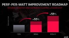
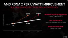
With its 7 nm RDNA architecture that debuted in July 2019, AMD achieved a nearly 50% gain in performance/Watt over the previous "Vega" architecture. At its 2020 Financial Analyst Day event, AMD made a big disclosure: that its upcoming RDNA2 architecture will offer a similar 50% performance/Watt jump over RDNA. The new RDNA2 graphics architecture is expected to leverage 7 nm+ (7 nm EUV), which offers up to 18% transistor-density increase over 7 nm DUV, among other process-level improvements. AMD could tap into this to increase price-performance by serving up more compute units at existing price-points, running at higher clock speeds.
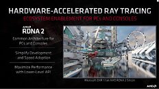
AMD has two key design goals with RDNA2 that helps it close the feature-set gap with NVIDIA: real-time ray-tracing, and variable-rate shading, both of which have been standardized by Microsoft under DirectX 12 DXR and VRS APIs. AMD announced that RDNA2 will feature dedicated ray-tracing hardware on die. On the software side, the hardware will leverage industry-standard DXR 1.1 API. The company is supplying RDNA2 to next-generation game console manufacturers such as Sony and Microsoft, so it's highly likely that AMD's approach to standardized ray-tracing will have more takers than NVIDIA's RTX ecosystem that tops up DXR feature-sets with its own RTX feature-set.Variable-rate shading is another key feature that has been missing on AMD GPUs. The feature allows a graphics application to apply different rates of shading detail to different areas of the 3D scene being rendered, to conserve system resources. NVIDIA and Intel already implement VRS tier-1 standardized by Microsoft, and NVIDIA "Turing" goes a step further in supporting even VRS tier-2. AMD didn't detail its VRS tier support.
AMD hopes to deploy RDNA2 on everything from desktop discrete client graphics, to professional graphics for creators, to mobile (notebook/tablet) graphics, and lastly cloud graphics (for cloud-based gaming platforms such as Stadia). Its biggest takers, however, will be the next-generation Xbox and PlayStation game consoles, who will also shepherd game developers toward standardized ray-tracing and VRS implementations.
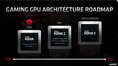
AMD also briefly touched upon the next-generation RDNA3 graphics architecture without revealing any features. All we know about RDNA3 for now, is that it will leverage a process node more advanced than 7 nm (likely 6 nm or 5 nm, AMD won't say); and that it will come out some time between 2021 and 2022. RDNA2 will extensively power AMD client graphics products over the next 5-6 calendar quarters, at least.


306 Comments on AMD RDNA2 Graphics Architecture Detailed, Offers +50% Perf-per-Watt over RDNA
(And again, please don't read this as me somehow saying that "Mark Papermaster is a genius that can only make brilliant decisions" - I am not arguing for something, I am arguing against your brash and unfounded assertions that these decisions are necessarily wrong. They might be wrong, but given AMD's recent history they might also be right. And unless you can present some actual basis for your claims, this is just wild speculation and entirely useless anyhow.)
Polaris production is winding down, current "production" is likely just existing chip inventories being sold out (including that new China-only downclocked "RX 590" whatsitsname). They are only competing directly as far as previous-gen products are still in the channel, which is a situation that takes a while to resolve itself every generation. Remember, the RX 5500 launched less than three months ago. A couple more months and supply of new Polaris cards will be all but gone.
But beyond that, you aren't talking about competitiveness, in fact I would say you aren't presenting a coherent argument for anything specific at all. What does an imagined delay from an imagined previous (2019?) launch date of Navi 2X have to do with competitiveness as long as it launches reasonably close to Nvidia's next generation and performs competitively? What does the lack of RTRT in Navi 1X have to do with competitiveness when there are currently just a handful of RTRT titles? If you want to make an overarching point about something, please make sure what you're talking about actually relates to that point.
Also, I forgot this one:4K TVs are mainstream because TV manufacturers need to sell new products and have spent a fortune on marketing a barely perceptible (at TV sizes and viewing distances) increase in resolution as a revolutionary upgrade. TVs are also not even close to mainly used or sold for gaming, they are TVs. 4k TVs being mainstream has nothing to do with gaming whatsoever.
Consoles can run 4k games because they turn down the image quality settings dramatically, and (especially in the case of the PS4 Pro) use rendering tricks like checkerboard rendering. They also generally target 30fps, at least at 4k. Console games generally run quality settings comparable to medium-low settings in their own PC ports. Digital Foundry (part of Eurogamer) has done a lot of great analyses on this, comparing various parts of image quality across platforms for a bunch of games. Worth the read/watch! But the point is, if you set your games to equivalent quality settings and lower your FPS expectations you can match any console with a similarly specced PC GPU. Again, DF has tested this too, with comparison images and frame time plots to document everything.That was what they said in the fin an day presentation, yeah, including specifically . This does make it seem like like RDNA (1) was a bit of a "we need to get this new arch off the ground" effort with lots of low-hanging fruit left in terms of IPC improvements. I'm mildly skeptical - it seems too good to be true - but saying stuff you aren't sure of at a presentation targeting the financial sector is generally not what risk-averse corporations tend to do. PR is BS, but what you say to your (future) shareholders you might actually be held accountable for.Not to mention at ~70W more power draw.
Also, if it is so straightforward, why does Intel struggle to roll out a competitive GPU?
The main differences between GCN and RDNA1 is GCN issues one instruction every 4 cycles. RDNA1 issues one instruction every 1 cycle. Also the wavefront size differs. GCN the wavefront is of 64 threads (Wave64). RDNA1 it's both 32 threads (Wave32) & 64 threads (Wave64). Even the multilevel cache has been greatly improved in RDNA1 over GCN.
UPDATE: I just read a few more of your posts. You already know what I posted. Ignore this :D .
It also comes from RDNA2 being a brand new architecture. Look at RDNA1 as a placeholder, to test the GPU waters and it did quite successfully.
RDNA2 is going to be a game changer IMO. :D
Product pls. The hype train crashed long ago.
they all get way too hot and only give 1440p performance . THE VEGA 64 Was supposed to be a game changer , but no.... the Bulldozer was junk and was the first time I changed to intel in 10 years
for 1 series of CPU ( Haswell ) . The new Ryzen seems to be going ok , lucky for them
I not sure about ur gaming , yet i could play bf4 at 1440 p no probs . Also Civ V with my R9 290 x XFX . Frickin Civ V has the freesync turned off for anti flickering with all vega64 and 5700xt cards for my system lol , no drivers have helped and ive tried them all.....
The new Ryzen seems to be going ok , lucky for them like I said, being a AMD die hard since AXIA 1000mhz days pal when AMD were the first to reach 1000 MHz . Also in AUS my Vega 64 was $900
and my 5700xt strix was $ 860 AUS , these are not cheap GPUs pal , and on top of it VEGA WAS running AT 90C , FULL GAME LOAD. AMD better pull there finger out for there next release or im out of there GPU segment
Still, I do hope the 50% perf/W number actually holds up, if so we should see both some seriously powerful big GPUs from AMD next go around, and likely some very attractive midrange options too.
I see RDNA2 as the ZEN2 or ZEN3 of GPUs.
From Amd/comments/ctfbemFigure 3 (bottom of page 5) shows 4 lines of shader instructions being executed in GCN, vs RDNA in Wave32 or “backwards compatible” Wave64.
Vega takes 12 cycles to complete the instruction on a GCN SIMD. Navi in Wave32 (optimized code) completes it in 7 cycles.
In backward-compatible (optimized for GCN Wave64) mode, Navi completes it in 8 cycles.
So even on code optimized for GCN, Navi is faster., but more performance can be extracted by optimizing for Navi.
Lower latency, and no wasted clock cycles.
For GCN wave64 mode, RDNA has about 33 percent higher efficiency when compared to Vega GCN, hence 5700 XT's 9.66 TFLOPS average yields around 12.8478 TFLOPS Vega II (real SKU has 14 TFLOPS). In terms of gaming performance, RX 5700 XT is very close to RX Vega II.
According to techpowerup,
RX 5700 XT has 219 watts average gaming while RX Vega II has 268 watts average gaming.
RX 5700 XT has 227 watts peek gaming while RX Vega II has 313 watts peek gaming.
Perf/watt improvements between RX 5700 XT and RX Vega II is about 27 percent. AMD's 50 percent perf/watt improvement between GCN to RDNA v1 is BS.
References
www.techpowerup.com/review/amd-radeon-rx-5700-xt/31.html
www.techpowerup.com/review/amd-radeon-vii/31.html
You need to keep in mind that the RX5700Xt is way smaller than RVII so not sure what you are measuring? If you go only for performance then ok but if you put power consumption vs performance then for the 5700 XT it will be lower but the performance as well due to CUs used in 5700XT compared to RVII. 2560 for 5700 Xt vs 3860 for VII. That is quite a lot in my book so it is not a BS as you said.
EDIT: Not to mention you are comparing card vs card not chip vs chip. HBM2 vs GDDR6 have also different power usage which you haven't included in your calculations.
It probably refers to the Navi model which have the largest gains over the previous model of similar performance or segment, whatever makes the most impressive metric. AMD, Intel, Nvidia, Apple, etc. are all guilty of doing this marketing crap.
But it doesn't mean that the whole lineup is 50% more efficient. People need to keep this in mind when they estimate Navi 2x, which is supposed to bring yet another "50%" efficiency, or rather up to 50% more efficiency.
2. I was referring to perf/watt.
3. GDDR6 (for 16 GBps 2.5w each x 8 chips) and HBM v2 (e.g `~20 watts Vega Frontier 16 GB) power consumption difference is minor when compared to GPUs involved.
16 GB HBM v2 power consumption is lower when compared to GDDR6 16 chip 16GB Clamshell Mode which is irrelevant for RX-5700 XT's 8 chips GDDR6-14000.
www.techpowerup.com/forums/threads/nvidias-next-generation-ampere-gpus-to-be-50-faster-than-turing-at-half-the-power.262592/
Nice features though, welcome to 2018.