Friday, March 6th 2020

AMD RDNA2 Graphics Architecture Detailed, Offers +50% Perf-per-Watt over RDNA
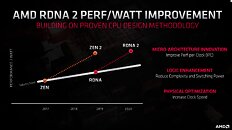
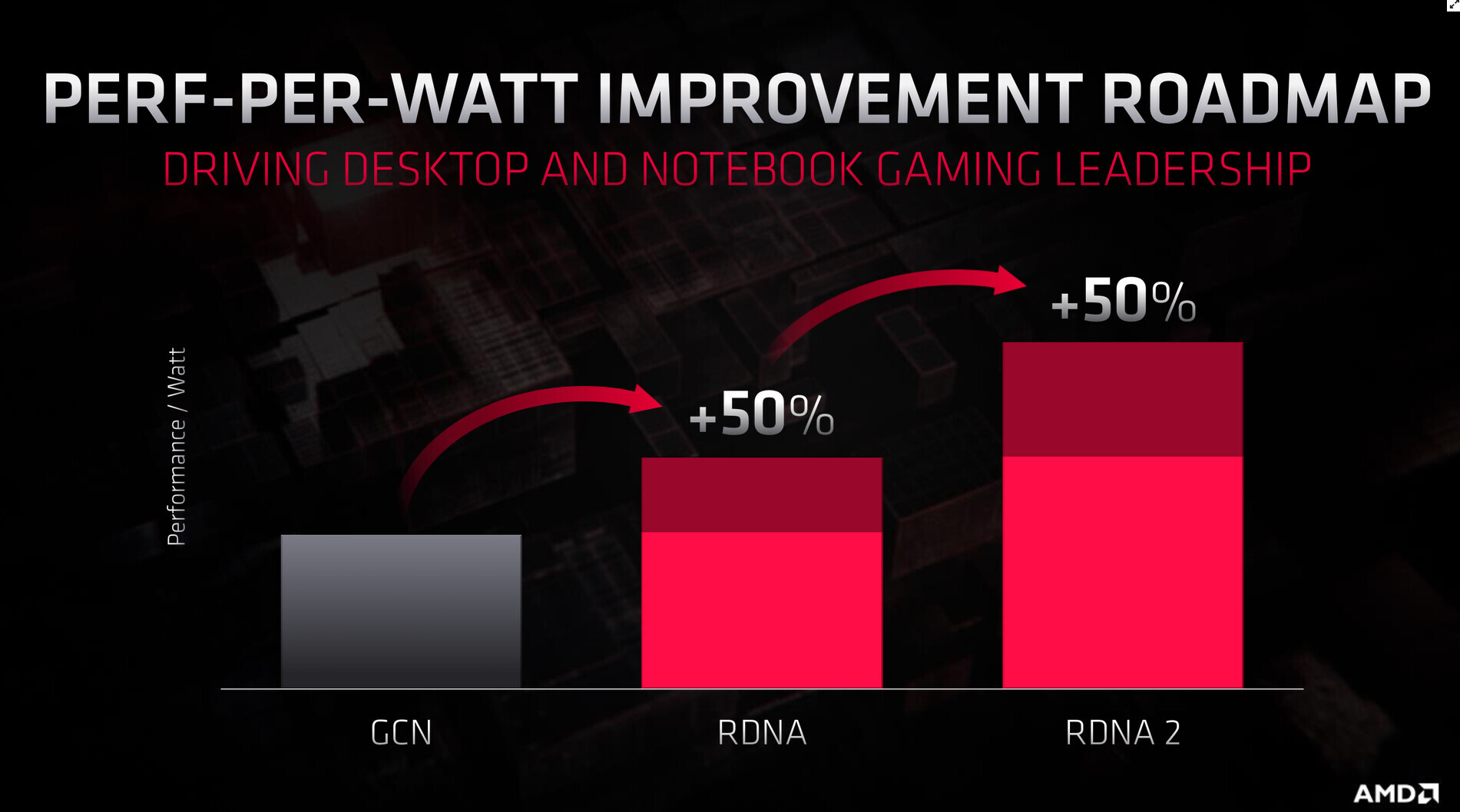
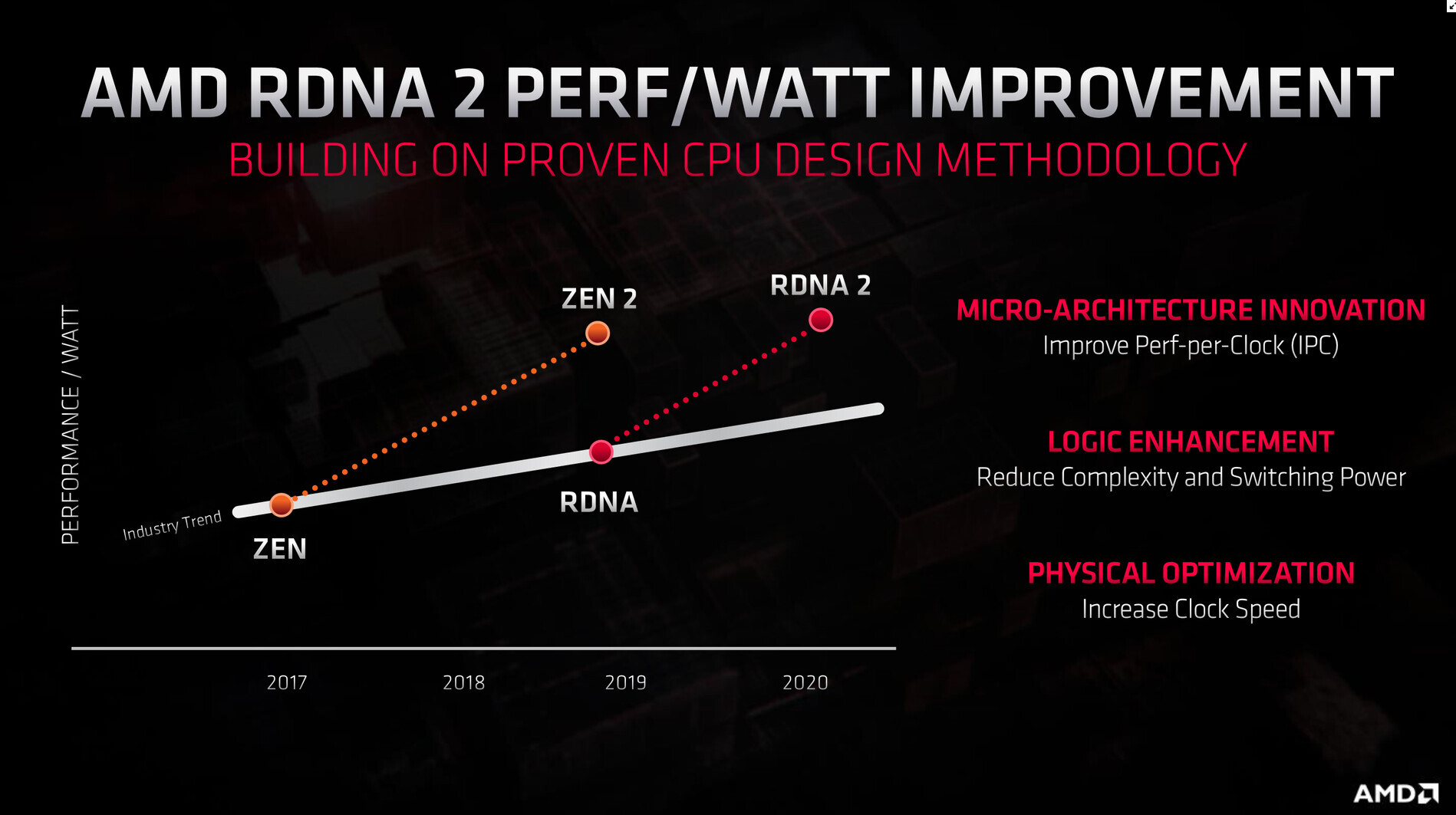
With its 7 nm RDNA architecture that debuted in July 2019, AMD achieved a nearly 50% gain in performance/Watt over the previous "Vega" architecture. At its 2020 Financial Analyst Day event, AMD made a big disclosure: that its upcoming RDNA2 architecture will offer a similar 50% performance/Watt jump over RDNA. The new RDNA2 graphics architecture is expected to leverage 7 nm+ (7 nm EUV), which offers up to 18% transistor-density increase over 7 nm DUV, among other process-level improvements. AMD could tap into this to increase price-performance by serving up more compute units at existing price-points, running at higher clock speeds.
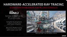
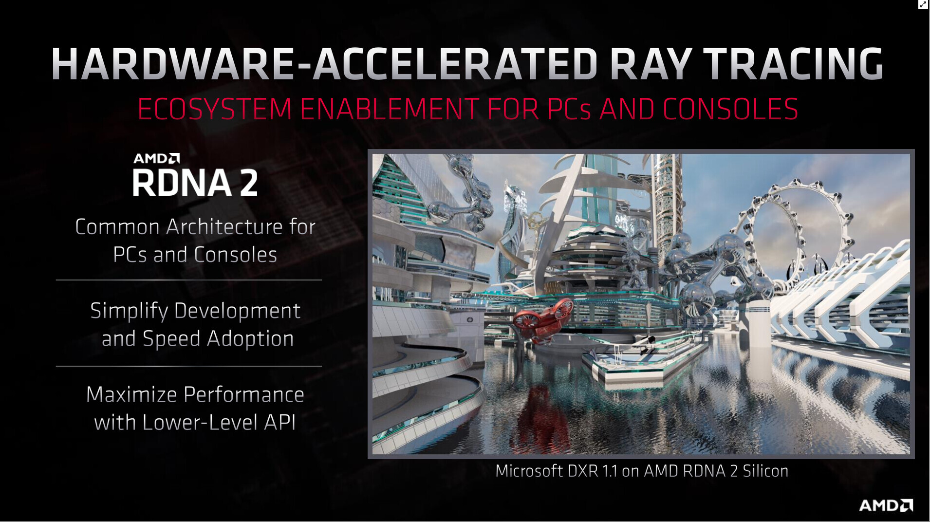
AMD has two key design goals with RDNA2 that helps it close the feature-set gap with NVIDIA: real-time ray-tracing, and variable-rate shading, both of which have been standardized by Microsoft under DirectX 12 DXR and VRS APIs. AMD announced that RDNA2 will feature dedicated ray-tracing hardware on die. On the software side, the hardware will leverage industry-standard DXR 1.1 API. The company is supplying RDNA2 to next-generation game console manufacturers such as Sony and Microsoft, so it's highly likely that AMD's approach to standardized ray-tracing will have more takers than NVIDIA's RTX ecosystem that tops up DXR feature-sets with its own RTX feature-set.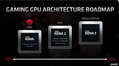

 Variable-rate shading is another key feature that has been missing on AMD GPUs. The feature allows a graphics application to apply different rates of shading detail to different areas of the 3D scene being rendered, to conserve system resources. NVIDIA and Intel already implement VRS tier-1 standardized by Microsoft, and NVIDIA "Turing" goes a step further in supporting even VRS tier-2. AMD didn't detail its VRS tier support.
AMD hopes to deploy RDNA2 on everything from desktop discrete client graphics, to professional graphics for creators, to mobile (notebook/tablet) graphics, and lastly cloud graphics (for cloud-based gaming platforms such as Stadia). Its biggest takers, however, will be the next-generation Xbox and PlayStation game consoles, who will also shepherd game developers toward standardized ray-tracing and VRS implementations.
AMD also briefly touched upon the next-generation RDNA3 graphics architecture without revealing any features. All we know about RDNA3 for now, is that it will leverage a process node more advanced than 7 nm (likely 6 nm or 5 nm, AMD won't say); and that it will come out some time between 2021 and 2022. RDNA2 will extensively power AMD client graphics products over the next 5-6 calendar quarters, at least.
AMD has two key design goals with RDNA2 that helps it close the feature-set gap with NVIDIA: real-time ray-tracing, and variable-rate shading, both of which have been standardized by Microsoft under DirectX 12 DXR and VRS APIs. AMD announced that RDNA2 will feature dedicated ray-tracing hardware on die. On the software side, the hardware will leverage industry-standard DXR 1.1 API. The company is supplying RDNA2 to next-generation game console manufacturers such as Sony and Microsoft, so it's highly likely that AMD's approach to standardized ray-tracing will have more takers than NVIDIA's RTX ecosystem that tops up DXR feature-sets with its own RTX feature-set.

AMD hopes to deploy RDNA2 on everything from desktop discrete client graphics, to professional graphics for creators, to mobile (notebook/tablet) graphics, and lastly cloud graphics (for cloud-based gaming platforms such as Stadia). Its biggest takers, however, will be the next-generation Xbox and PlayStation game consoles, who will also shepherd game developers toward standardized ray-tracing and VRS implementations.
AMD also briefly touched upon the next-generation RDNA3 graphics architecture without revealing any features. All we know about RDNA3 for now, is that it will leverage a process node more advanced than 7 nm (likely 6 nm or 5 nm, AMD won't say); and that it will come out some time between 2021 and 2022. RDNA2 will extensively power AMD client graphics products over the next 5-6 calendar quarters, at least.
306 Comments on AMD RDNA2 Graphics Architecture Detailed, Offers +50% Perf-per-Watt over RDNA
Makes me rather curious to see the sizes of RDNA2 GPUs for PC.
wccftech.com/amd-radeon-rx-navi-21-gpu-2x-performance-5700-xt-die-size-rumor/
The density gains of the XSX would indicate more than 1:1 scaling from Navi 10, i.e. a 505mm2 chip would either have >80 CUs or some other stuff added on that we don't yet know about. Let's look closer at this.
Navi 10 has 40 CUs, a 256-bit G6 bus and a single IF/PCIe 4.0 x16 link on a 251mm² die. The XSX die is 360mm² with 56 CUs, 8 Zen 2 cores, and I/O including a 320-bit G6 bus. A Zen 2 CCD is 74 mm² with two 31.3 mm² CCXes,16MB of L3, IF links and anything else that lives on that die. Let's be conservative and discount L3 completely - the XSX then uses at least 2x31.3 mm² = 62.6mm² of die area to its CPU cores (likely a bit more as it won't have zero L3 cache, but will also likely gain density from the node improvement. Some space will also be used for the IF links between the CPU, GPU and memory controllers). This leaves us with at most 360mm² - 63mm² = 297mm² for
5256 CUs, all encode/decode blocks (which given the importance of streaming are likely to be fully featured and not cut down), a 320-bit GDDR6 PHY + controllers (compared to the 256-bit PHY and controllers of Navi 10, so 25% more die area for that), and at least two PCIe links for SSDs (unknown whether these are PCIe 3.0x4, PCIe 4.0x2 or PCIe 4.0x4 at this point), plus the chipset uplink etc. While the XSX does gain something in having slightly less I/O than a PC GPU, the gains from that are minor at best. Ignoring that, we have a 25% increase in VRAM die area + a30%40% increase in CUs with just an ~18% increase in die size (with the CPU subtracted, that is). And that includes RT hardware.While this is some real napkin math (we have no idea if anything beyond the die sizes here is actually accurate in terms of numbers, but IMO they shouldn't be too far off), it tells us that a 505mm² RDNA 2 GPU on the same improved 7nm node as the XSX either must have more than 80 CUs - if the scaling roughly follows my calculations a 100% area increase would then be more like a 120% increase in CUs, or ~95 CUs - or use a lot of die area for something else. Might we see significantly more RT power compared to shader pwerformance in the PC GPUs? Also, if it uses HBM2 rather than a stupidly large 512-bit G6 bus (which IMO sounds likely, despite what that BBS post says), the CU count could grow further (100?) as HBM controllers and PHYs are much more space efficient than G6.
Still, with all of this within the realm of IMO reasonable speculation (and it is very much speculation at this point) we have no idea about power, clocks, or anything else. Performance would vary wildly based on all of this. Pricing is also crucial, and a 505mm2 die on TSMC 7nm is not going to be cheap. So, as I've said both here and elsewhere, I don't see a reason to doubt that AMD can bring about a true flagship this generation, but both the absolute performance and pricing is entirely up in the air at this point, as is its competitiveness with Nvidia's so far entirely unknown Ampere arch. There's absolutely no indication in any of this that this will beat Ampere, simply because Ampere is entirely unknown. But will it be powerful? Absolutely.
Edit: I borked my numbers from about halfway through by calculating from the 52 active CUs in the XSX die rather than the 56 physically present ones. Fixed that; also added a note about possibly using "free" die space for more RT power compared to consoles.
I am quite sure that IF AMD wants to be competitive, they will design the Navi 2 GPU to be in line performance-wise with what comes next after Turing.
I mean it should be easy for them to take all the data they can gather on the previous generations and calculate an appropriate performance window range where the Turing successor will likely fall.
They did it with Zen. And they said that Zen targets the performance level where they expected Skylake-next-gen to be.
I mean, sure, AMD has obviously been working on their next flagship GPU based on an estimate of where Nvidia's competing architecture will be in terms of performance. But so what? They're still going to make the best products they can within the constraints of die size/cost/power/thermals for the high end, with everything else being spaced downwards to be competitive while producing sufficient margins and selling well. Only pricing (and thus margins) and the specifics of cut-down SKUs is really dependent on the competition.
The next-gen XBox will do 380 billion:
"the hardware acceleration for ray tracing maps traversal and intersection of light at a rate of up to 380 billion intersections per second"
www.eurogamer.net/articles/digitalfoundry-2020-inside-xbox-series-x-full-specs
Specs (all clocks are fixed, silicon is custom):
- 12.155 TFLOPs
- AMD Zen 2 8c/16t @ 3.6-3.8 Ghz - Hyperthreading can be disabled for a 3.8 Ghz clock or enabled for a 3.6 ghz clock
- 16 GB GDDR6 ECC (!!!)
- 52 CU 3328 Shader GPU @ 1,825 MHz
- Memory bandwidth: 10GB at 560GB/s, 6GB at 336GB/s
- 7nm - NOT EUV
- 1TB NVME SSD storage
Amd/comments/fjkkev... and Nvidia is still on 12nm.
The 5700XT is based on RDNA1. The upcoming RDNA2 is far more efficient. The XboxSX shows how efficient and fast it is, and that's a limited sample size APU. Lol
Nvidia should see a massive efficiency lift from 12nm all the way down to 7nm and some claim even 10nm and 8nm.
www.guru3d.com/news-story/rumor-nvidia-geforce-ampere-to-be-fabbed-at-10nmall-cards-rtx.html
I'm sure you already knew this too. It's all about Next Generation Gaming Consoles.
I bet it REALLY has more efficiency than the generation before that too!!! lol
www.tomshardware.com/reviews/nvidia-turing-gpu-architecture-explored,5801-10.html
According to sources and AMD themselves, RDNA2 is a architecture overhaul. What does Nvidia's GPU architecture have to do with RDNA2? Absolutely nothing lol, but you seem to be a little confused or too Nvidia biased. To each there own I suppose. I'll follow the evidence, you can continue to follow the fantasies.
Lol fantasies...lolololwtfbbqfanboysos
It's like groundhog day with you, lol.