Friday, March 6th 2020

AMD RDNA2 Graphics Architecture Detailed, Offers +50% Perf-per-Watt over RDNA
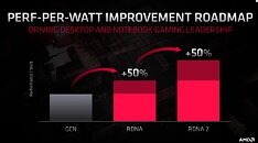
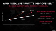
With its 7 nm RDNA architecture that debuted in July 2019, AMD achieved a nearly 50% gain in performance/Watt over the previous "Vega" architecture. At its 2020 Financial Analyst Day event, AMD made a big disclosure: that its upcoming RDNA2 architecture will offer a similar 50% performance/Watt jump over RDNA. The new RDNA2 graphics architecture is expected to leverage 7 nm+ (7 nm EUV), which offers up to 18% transistor-density increase over 7 nm DUV, among other process-level improvements. AMD could tap into this to increase price-performance by serving up more compute units at existing price-points, running at higher clock speeds.
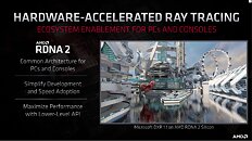
AMD has two key design goals with RDNA2 that helps it close the feature-set gap with NVIDIA: real-time ray-tracing, and variable-rate shading, both of which have been standardized by Microsoft under DirectX 12 DXR and VRS APIs. AMD announced that RDNA2 will feature dedicated ray-tracing hardware on die. On the software side, the hardware will leverage industry-standard DXR 1.1 API. The company is supplying RDNA2 to next-generation game console manufacturers such as Sony and Microsoft, so it's highly likely that AMD's approach to standardized ray-tracing will have more takers than NVIDIA's RTX ecosystem that tops up DXR feature-sets with its own RTX feature-set.Variable-rate shading is another key feature that has been missing on AMD GPUs. The feature allows a graphics application to apply different rates of shading detail to different areas of the 3D scene being rendered, to conserve system resources. NVIDIA and Intel already implement VRS tier-1 standardized by Microsoft, and NVIDIA "Turing" goes a step further in supporting even VRS tier-2. AMD didn't detail its VRS tier support.
AMD hopes to deploy RDNA2 on everything from desktop discrete client graphics, to professional graphics for creators, to mobile (notebook/tablet) graphics, and lastly cloud graphics (for cloud-based gaming platforms such as Stadia). Its biggest takers, however, will be the next-generation Xbox and PlayStation game consoles, who will also shepherd game developers toward standardized ray-tracing and VRS implementations.
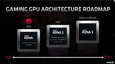
AMD also briefly touched upon the next-generation RDNA3 graphics architecture without revealing any features. All we know about RDNA3 for now, is that it will leverage a process node more advanced than 7 nm (likely 6 nm or 5 nm, AMD won't say); and that it will come out some time between 2021 and 2022. RDNA2 will extensively power AMD client graphics products over the next 5-6 calendar quarters, at least.


306 Comments on AMD RDNA2 Graphics Architecture Detailed, Offers +50% Perf-per-Watt over RDNA
That's a comparison against Vega10. Then the slides show 50% more against RDNA 1. Without any process improvements eh?
I predict we'll see a 386bit memory Navi. Navi is bandwidth starved at the moment.
When the R9's came out I was stoked. I still have my R9 290 from 2013 and it still can handle most games at 1440p with some settings turned down. I was very disappointed with the Polaris architecture. All they did was make them more power efficient with the same performance as my 290. Hell, my 290 still beats the RX580 in some benchmarks... I am looking forward to getting a 5700XT when the new cards drop though :)
The 5700XT was... Well a 2070 killer and a 2070 Super fighter.
It'll be nice if AMD can finally field another Radeon that can actually challenge for the performance crown again.
How long has it been since the Fury X came out? :-(I really don't see how AMD can get a 50% boost over RDNA 1 without a new and wider memory controller.
The 5700XT is desperately starved for bandwidth.
It's like my modified Fury X. Tightened up the HBM timings and at stock speed I can get over 300GB/s in OCLMembench. Stock as a rock the Fury X gets between 180-220GB/s for memory bandwidth. At 500mhz or well DDR for 1000 effective, it's theoretical is at 512GB/s.
It's hard for me to compare apples to apples because the mods also undervolted and under-clocked the core. Though it's similar with the 5700 XT... You can get nearly the same performance with less power by undervolting and mild under-clocked.
Either way a Fury X at 1000/1000 blows the doors off one at 1050/1000. On stock bios and I need to push the volts but it takes 1150/1200 to match.
It burns a lot more power. Tuned up makes a much happier Fury X that gets a significant bump to perf vs watts.
So if AMD could just not have to bring their damn architecture for every clock, it's possible to get most of the way there.
Which is why I think...
A refined 5700XT with 384bit memory that drops even 1-200mhz core from where it is now with a matching drop in vcore. That's not adding any other extra transistors to the die. Bump it to 44 CUs from 32, drop the core clocks 2-400mhz... All the way there.
Look at the 2080 Ti vs the 2080 Super. Bigger silicon, significantly less clocks, but it still performs.
Even if you go back more than a decade to the times of northbridges, ATI was the worst (while nVidia was the best at maximizing bandwidth). Nothing has changed.
Often reviewers site that nVidia designs are more memory bandwidth efficient, but while this might be true, my guess is that nVidia just gets more effective bandwidth out of the memory.
Instruction throughput is not indicative of performance because that's not how GPUs extract performance. Let's say you want to perform one FMA over 256 threads, with GCN5 you'd need 4 wavefronts that would take 4 clock cycles within one CU, with RDNA you'd need 8 wavefronts which would also take the same 4 clock cycles within one CU. The same work got done within the same time, it wasn't faster in either case.
Thing is, it takes more silicon and power to schedule 8 wavefronts instead of 4 so that actually makes GCN more efficient space and power wise, if you've ever wondered why AMD would always be able to fit more shaders within the same space and TDP than Nvida, that's how they did it. And that's also probably why Navi 10 wasn't as impressive power wise as some expected and why it had such a high transistor count despite it not having any RT and tensor hardware (Navi 10 and TU106 practically have the same transistor count).
But as always there's a trade off, a larger wavefront means more idle threads when a hazard occurs such as branching. Very few workloads are hazard-free, especially a complex graphics shader, so actually in practice GCN ends up being a lot more inefficient per clock cycle on average.
Again, RDNA2 is NOT competing with Nvidia's current generation graphics. Which is why there was some patents out about a possible RX 5800XT & 5900XT based on a revamped RDNA1 as a placeholder until RDNA2 is released by the beginning of Q4 2020. Or these revamps could be RDNA2, despite that gen being called RX 6000 series.
They also need full support of the latest HDMI and DisplayPort interfaces - HDMI 2.1 and DP 2.0.
50% performance/watt improvement is good - it means a card at 150 W which renders a game with 100 FPS, will now render it with 150 FPS.
RDNA 1.0 is just a hybrid, it keeps GCN characteristics.
In fact if you look throughout the history of GPUs you'll see that most of the performance typically comes from more shaders and higher clockspeeds, that's pretty much the number one driving factor for progress by far.
RDNA 2.0 will have ray-tracing hardware and variable rate shading capability which on their own should rearrange the architecture even further.
VLIW5 - VLIW4 - GCN:
Radeon HD 7870 Pitcairn GCN 1.0 original:
Radeon RX Vega GCN 1.4 vs Radeon RX 5700 XT RDNA 1.0 original:
I even searched it and "Ati Chipsets" was right there and it didn't even register. lol