Thursday, February 13th 2025

AMD to Build Next-Gen I/O Dies on Samsung 4nm, Not TSMC N4P
Back in January, we covered a report about AMD designing its next-generation "Zen 6" CCDs on a 3 nm-class node by TSMC, and developing a new line of server and client I/O dies (cIOD and sIOD). The I/O die is a crucial piece of silicon that contains all the uncore components of the processor, including the memory controllers, the PCIe root complex, and Infinity Fabric interconnects to the CCDs and multi-socket connections. Back then it was reported that these new-generation I/O dies were being designed on the 4 nm silicon fabrication process, which was interpreted as being AMD's favorite 4 nm-class node, the TSMC N4P, on which the company builds everything from its current "Strix Point" mobile processors to the "Zen 5" CCDs. It turns out that AMD has other plans, and is exploring a 4 nm-class node by Samsung.
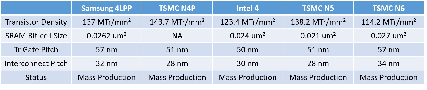
This node is very likely the Samsung 4LPP, also known as the SF4, which has been in mass-production since 2022. The table below shows how the SF4 compares with TSMC N4P and Intel 4, where it is shown striking a balance between the two. We have also added values for the TSMC N5 node from which the N4P is derived from, and you can see that the SF4 offers comparable transistor density to the N5, and is a significant improvement in transistor density over the TSMC N6, which AMD uses for its current generation of sIOD and cIOD. The new 4 nm node will allow AMD to reduce the TDP of the I/O die, implement a new power management solution, and more importantly, the need for a new I/O die is driven by the need for updated memory controllers that support higher DDR5 speeds and compatibility with new kinds of DIMMs, such as CUDIMMs, RDIMMs with RCDs, etc.
Sources:
The Bell, Jukanlosreve (Twitter)
This node is very likely the Samsung 4LPP, also known as the SF4, which has been in mass-production since 2022. The table below shows how the SF4 compares with TSMC N4P and Intel 4, where it is shown striking a balance between the two. We have also added values for the TSMC N5 node from which the N4P is derived from, and you can see that the SF4 offers comparable transistor density to the N5, and is a significant improvement in transistor density over the TSMC N6, which AMD uses for its current generation of sIOD and cIOD. The new 4 nm node will allow AMD to reduce the TDP of the I/O die, implement a new power management solution, and more importantly, the need for a new I/O die is driven by the need for updated memory controllers that support higher DDR5 speeds and compatibility with new kinds of DIMMs, such as CUDIMMs, RDIMMs with RCDs, etc.
65 Comments on AMD to Build Next-Gen I/O Dies on Samsung 4nm, Not TSMC N4P
Hopefully rumours are true and the packaging takes a huge jump to mitigate the same issue Zen has had since it's first generation.
It isn't *just* Apple, but they're kind of made for and dictated by Apple, so I guess that's why I say that. You're right it's not *just* them, though. There are other mobile chips (that generally flip nodes at same time).
SDEG2 is N3P (they tried Samsung but apparently it sucked too much and/or couldn't yield). SDEG3 they *want* to be on Samsung 2nm, but like I said, I think everyone is waiting to see if Samsung can do it.
Did we say this about 3nm? Yes we did. Were they able to do it? No they weren't. Will it be different this time? I don't know. :p
More than that and you're better off with HPC anyway.
Don't act like use cases for >128GBs don't exist. I know there is HEDT but still, options. Options should be there.
I'm running 128GBs right now for one very high ram use case.
From what I understand they could add support via a BIOS update, they just haven't. Perhaps there's not much need considering the promised 64 GB CUDIMMs haven't materialised anyway.
But again, the MT cap isn't limited by the IMC, at least not for 2 DIMM, it's limited by IF having to stay in sync, which is capped by the chiplet design and cheap packaging.
Zen 4 above & Zen 5 below ~
old.chipsandcheese.com/2024/11/24/pushing-amds-infinity-fabric-to-its-limits
Sure, TSMC N4 would be a better choice.
Zen 6 12-core CCD is reportedly gonna be made using TSMC N3 process, which should allow for achieving similar size as does 12-cores in Strix Point already made using TSMC N4. TSMC N3 has about 55% higher density than TSMC N4, which is something that should allow AMD to achieve 12 full Zen 6 cores (incl. 48 MB L3 cache) per CCD. Anyway, AMD really needs more cores per CCD to stay competitive, as Intel keeps raising cores.
If AMD stays with 8 cores per CCD in Zen 6, that's gonna be a total disaster. Since Zen 5 is already AVX-512 focused generation with improved caches and prediction algorithm, I can't think of anything else but increasing cores with Zen 6 to increase performance enough.
You can't seriously believe they'd make something to threaten low end TR or EPYC do you?
I agree that hopefully they have some better packaging because the current limits on bandwidth are dashing the advantage AMD has in latency for bursty workloads.
I'm not complaining. Honestly AM5 still does what I need. But I do see spots for improvement.
If what they said about strix halo having insane IF bandwith is true (i presume just doubling the connections) AMD could be doing the same with this rumored 4nm IOD.