Thursday, February 13th 2025

AMD to Build Next-Gen I/O Dies on Samsung 4nm, Not TSMC N4P
Back in January, we covered a report about AMD designing its next-generation "Zen 6" CCDs on a 3 nm-class node by TSMC, and developing a new line of server and client I/O dies (cIOD and sIOD). The I/O die is a crucial piece of silicon that contains all the uncore components of the processor, including the memory controllers, the PCIe root complex, and Infinity Fabric interconnects to the CCDs and multi-socket connections. Back then it was reported that these new-generation I/O dies were being designed on the 4 nm silicon fabrication process, which was interpreted as being AMD's favorite 4 nm-class node, the TSMC N4P, on which the company builds everything from its current "Strix Point" mobile processors to the "Zen 5" CCDs. It turns out that AMD has other plans, and is exploring a 4 nm-class node by Samsung.
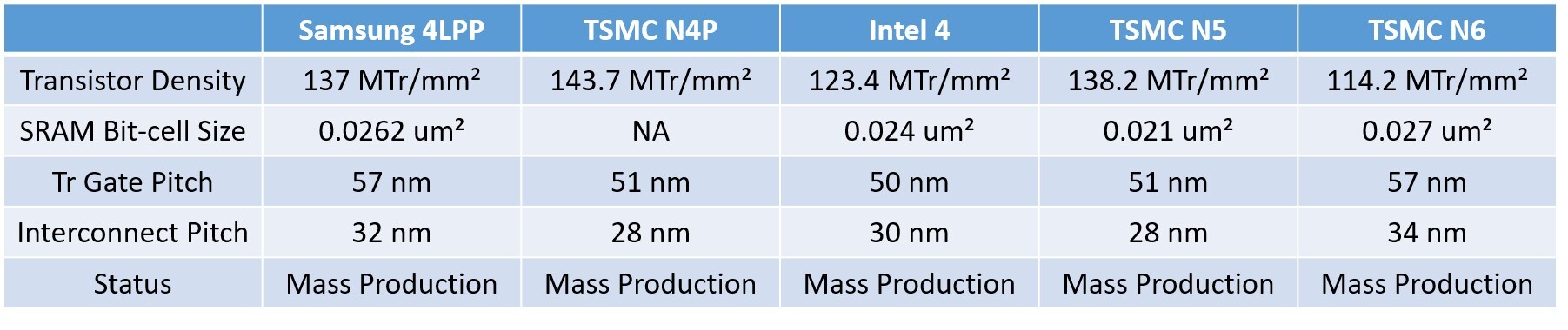
This node is very likely the Samsung 4LPP, also known as the SF4, which has been in mass-production since 2022. The table below shows how the SF4 compares with TSMC N4P and Intel 4, where it is shown striking a balance between the two. We have also added values for the TSMC N5 node from which the N4P is derived from, and you can see that the SF4 offers comparable transistor density to the N5, and is a significant improvement in transistor density over the TSMC N6, which AMD uses for its current generation of sIOD and cIOD. The new 4 nm node will allow AMD to reduce the TDP of the I/O die, implement a new power management solution, and more importantly, the need for a new I/O die is driven by the need for updated memory controllers that support higher DDR5 speeds and compatibility with new kinds of DIMMs, such as CUDIMMs, RDIMMs with RCDs, etc.
Sources:
The Bell, Jukanlosreve (Twitter)
This node is very likely the Samsung 4LPP, also known as the SF4, which has been in mass-production since 2022. The table below shows how the SF4 compares with TSMC N4P and Intel 4, where it is shown striking a balance between the two. We have also added values for the TSMC N5 node from which the N4P is derived from, and you can see that the SF4 offers comparable transistor density to the N5, and is a significant improvement in transistor density over the TSMC N6, which AMD uses for its current generation of sIOD and cIOD. The new 4 nm node will allow AMD to reduce the TDP of the I/O die, implement a new power management solution, and more importantly, the need for a new I/O die is driven by the need for updated memory controllers that support higher DDR5 speeds and compatibility with new kinds of DIMMs, such as CUDIMMs, RDIMMs with RCDs, etc.
65 Comments on AMD to Build Next-Gen I/O Dies on Samsung 4nm, Not TSMC N4P
I think if people can max out Cas32/34 with something like this they'll be plenty happy.
FWIW, 7200mhz would already essentially negate the purpose of X3D of 8-core chips, more-or-less, which is likely why AMD is moving to 12-core CCDs.
Like-wise, the newer memory controller *should* essentially increase PPC on the normal architecture quite a bit, which is something a new generation needs and this generation didn't really have.
This is the reason why Ryzen CPUs are 20-25W higher idle than Intel from what I understand:
tpucdn.com/review/amd-ryzen-7-9800x3d/images/power-idle.png
Leveraging one of the benefits of their chiplet design, more margin early in lifecycle, deeper discounts later in the lifecycle. Everyone wins.
Also they will start gaining experience on Samsung's nodes, meaning, later they could transition some of their chips on Samsung's fabs. The next UDNA series could have low end GPUs on Samsung nodes and mid - hopefully - high end GPUs on TSMC nodes. A 130W low end GPU made by Samsung instead of a 110W low end GPU made by TSMC, wouldn't be a dissaster, for example. It will mean more waffers for those mid-high end GPUs made by TSMC. Considering TSMC is also increasing prices, this migth be necessary.
I've gotta believe they'll go from supporting 6000->7200mhz(+), and even if Samsung is only 20% that's fine. Realistically it would be what, ~6200/6300->~7600mhz?
Even if they only can guarantee CL30/6400 or CL32/6800 that would still be okay. The lack of guaranteed CL30/6400 really hurts them the most, imho.
DGMW, I'd love to see 8000mhz(+) support, maybe a 4x ratio instead of 3x, and even CUDIMMs, and hope we do.
I just wonder if they really want that given they make a ton of money selling V-cache parts and the higher memory scales the less attractive they will look.
But again, 12 cores instead of 8...so idk. We'll have to see what they do wrt inherent cache structure as well as v-cache (amount) to see what really makes the most sense and what their plan is going to be.This is a fair point. While TSMC gets the press, there will reach a point where inevitably Samsung (heck, even Rapidus) will have decent 2nm output and likely quality.
Never hurts to prepare. I'm not saying they'll be better, I'm not saying they'll have the same volume...but you're right to say it's good to be prepared to have the option.
Getting familiar with how their SDK/nodes work is not a bad idea, even if starting with something small/more-simple such as like this.
I don't get the analogy of not using TSMC N4P so it frees up N3E/N2 space. :p
I hear ya, tho. I'm not judging. Like I said; I think they need an improvement over what they have, but also don't need anything super drastic, so Samsung is okay if it gives at least some tangible improvement.
If we get a 4x IF 1:1 ratio (so essentially 8000mhz support) that would be cool. And while I want and think we will get ~7200-7600mhz support, even 6400-6800mhz support would be an upgrade.
As I've said, it's been pretty clear AMD has been dragging their feet on the MC to accentuate v-cache parts. Whatever they do to nix that limitation on non v-cache chips is good.
I'm hoping, given the switch to 12-core CCDs, the memory limitation instances of 6-8 cores is all but eliminated so they can shift the bottleneck to v-cache instead feeding 50% more cores.
This would help PPC of Zen 6 look much better than Zen 4->Zen 5, even if essentially just shifting current v-cache improvement into an arch upgrade, which I would argue is something they need to finally do.
www.techpowerup.com/cpu-specs/ryzen-9-7950x.c2846
Don't go just by enthusiast forums, as long as AMD makes them smaller nodes will be relevant & when they move someone else will fill in their place who doesn't need $20k bleeding edge wafers!
Samsung 2nm monolithic for desktop or not buying. 122+70 single die. what's the problem.
Last I heard Zen 6 was planned to be N3E and Zen 6c was N2/N3E depending on market. I don't think this has changed? :confused:Thanks for the refresher on the IOD density...I'll have to figure out exactly what that translates to for analog (vs other processes) when I have time.
Are you curious about density of 5070? I figure it's bc it's aimed to clocked higher (by relaxing density). I've been trying to explain that to people...prolly a special child...and likely a design test for clocks on 3nm.
Less units; higher clock; same POS 4070ti under a new configuration (but similar die size). Lipstick on a pig, I do 'reckon. Will it fool the cattle? :p
FWIW, N48 is also kinda that. I would not be surprised if either and/or both of them are more-or-less ported to 128-bit/192-bit 3nm designs, and/or if both of them started as 3nm before it got delayed.
FWIW, I've also been arguing for a while that if Samsung can get their 2nm (not early 2nm which is actually like N3P, but actual 2nm) yields up that AMD should seriously consider them. On that we agree.
Granted, my reason for that is if they go to chiplets for gfx, they could essentially make everything at Samsung (bc everything would be under ~100mm2)...shouldn't be hard to yield...but that's a different topic.
Maybe it will save some 5nm TSMC for the next gen IO die, but then the 5nm will not be widely used so same story as freeing 6nm.
It is only financial move and I doubt we will see lower price for the next gen hardware, maybe we won't see price increase, but the shift to Samsung for the IO die will hurt the performance of the memory controller and the power consumption for sure
www.techpowerup.com/cpu-specs/ryzen-5-7535hs.c3042
www.techpowerup.com/cpu-specs/ryzen-5-6600u.c2522
They're still being made & sold even now.Those would probably be EPYC's only, the zen 5(c?) based EPYC are on better nodes as well. We'll need to wait till the actual chips come out though so who knows maybe AMD will surprise us?
www.techpowerup.com/cpu-specs/epyc-9965.c3904
www.techpowerup.com/cpu-specs/ryzen-9-9950x.c3649
The reason I figure there has to be also Zen 6c on N3E (and not just 2nm Epyc) is because I doubt the PS6 SOC will be 2nm. Unless they use the Turin design, which they might, that has to be available elsewhere.
Because that's how these things work. AMD kinda slaps their existing designs together to make SOCs. So whatever they plan for N3E, that's what Sony can/will use. Makes sense it would be available in laptop.
I really doubt Sony would use a full-blood Zen 6 when a 'C' design makes a lot more sense for their use-case. That's why the ? is if it's like Turin or rather a 6c on N3.
For instance, the M5 just started MP on N3P. We can expect this same thing to occur next year but on N2. This is when mass production for everything else (Zen6/UDNA/prolly Rubin) will occur on N3E.
But yes, as far as 2nm goes...I agree. Has to only be something like Turin where margins are astronomical for the reasons you stated. This is why 2nm Samsung might make sense for future consumer products.
It will be interesting to see how Samsung yields go, performance is, and how quickly they are able to improve 2nm vs N3P. That's how/why Samsung *could* be a potential choice for future consumer CPU/GPUs.