Thursday, February 13th 2025

AMD to Build Next-Gen I/O Dies on Samsung 4nm, Not TSMC N4P
Back in January, we covered a report about AMD designing its next-generation "Zen 6" CCDs on a 3 nm-class node by TSMC, and developing a new line of server and client I/O dies (cIOD and sIOD). The I/O die is a crucial piece of silicon that contains all the uncore components of the processor, including the memory controllers, the PCIe root complex, and Infinity Fabric interconnects to the CCDs and multi-socket connections. Back then it was reported that these new-generation I/O dies were being designed on the 4 nm silicon fabrication process, which was interpreted as being AMD's favorite 4 nm-class node, the TSMC N4P, on which the company builds everything from its current "Strix Point" mobile processors to the "Zen 5" CCDs. It turns out that AMD has other plans, and is exploring a 4 nm-class node by Samsung.
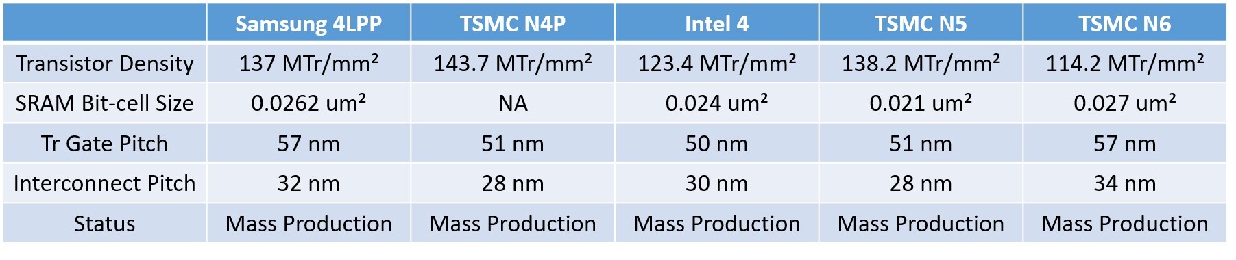
This node is very likely the Samsung 4LPP, also known as the SF4, which has been in mass-production since 2022. The table below shows how the SF4 compares with TSMC N4P and Intel 4, where it is shown striking a balance between the two. We have also added values for the TSMC N5 node from which the N4P is derived from, and you can see that the SF4 offers comparable transistor density to the N5, and is a significant improvement in transistor density over the TSMC N6, which AMD uses for its current generation of sIOD and cIOD. The new 4 nm node will allow AMD to reduce the TDP of the I/O die, implement a new power management solution, and more importantly, the need for a new I/O die is driven by the need for updated memory controllers that support higher DDR5 speeds and compatibility with new kinds of DIMMs, such as CUDIMMs, RDIMMs with RCDs, etc.
Sources:
The Bell, Jukanlosreve (Twitter)
This node is very likely the Samsung 4LPP, also known as the SF4, which has been in mass-production since 2022. The table below shows how the SF4 compares with TSMC N4P and Intel 4, where it is shown striking a balance between the two. We have also added values for the TSMC N5 node from which the N4P is derived from, and you can see that the SF4 offers comparable transistor density to the N5, and is a significant improvement in transistor density over the TSMC N6, which AMD uses for its current generation of sIOD and cIOD. The new 4 nm node will allow AMD to reduce the TDP of the I/O die, implement a new power management solution, and more importantly, the need for a new I/O die is driven by the need for updated memory controllers that support higher DDR5 speeds and compatibility with new kinds of DIMMs, such as CUDIMMs, RDIMMs with RCDs, etc.
65 Comments on AMD to Build Next-Gen I/O Dies on Samsung 4nm, Not TSMC N4P
7600 (6nm, 32MB cache) = 65MTr/mm²
4060 Ti (5nm custom, 32MB cache) = 121.8MTr/mm²
The transistor density of the 6nm client I/O die from "Raphael/Zen5" is approximately 27.87mTr/mm²
Samsung's 4nm process is already in its third or fourth iteration and is now very close to the competition in both yields and density. I see this as a positive move; Samsung is likely offering a significant discount, and AMD will have the opportunity to address one of Zen 5's biggest shortcomings, the IOD and Memory controller.
randomsexperts here, to tell its engineers why they shouldn't use samsung's node on its next io die.It's quite obvious both companies have a partnership and this move would end up benefitting both, whilst freeing up capacity at tsmc for the more advanced nodes.
Maybe the crowd here isn't as bad as you think!
As for the memory support, the performance and all that, the key point would probably be if they use the new fanout interconnection of Halo or what they use on RDNA3 or if they continue to use Infinity fabrics + SerDes like the current lineup. Just moving to the new fanout thing will remove the latency of serializing and deserialising the data over the infinity fabrics.
But in reality, as much as the hardware enthusiast in me would like to have the best I/O die possible that would scale to infinity and all that, in reality, most of the people probably overstate the importance of the I/O die for real world performance. The "Crappy" Zen 4/5 I/O die still is in the best desktop CPU in the market.
Doing a design is always about tradeoff. You can put a bit more of this and that, but that will bring more of this and that. You win when you are able to get the best compromise. Performance is a thing, but production cost is another. And there plenty of other tradeoff to consider.
We will see but i am not worried. Still intriged about the CCD. I think that is what really matter anyway. Having a good core is crucial.
1. new, faster Infinity Fabric PHY. It will be either classic upgrade to 'GMI4' or a new solution used on Strix Halo die
chipsandcheese.com/p/amds-strix-halo-under-the-hood
2. maybe more PCIe lanes, hopefully one extra x4, in total 32 lanes, just like IOD on Zen2/3 had (not all lines were enabled)
3. new and faster IMC, possibly ~6800/7200 MT/s
4. new iGPU with either 2CUs or 4CUs; RDNA4?
5. new VCN media engine with better encoders and codec support
6. new DCN display engine; native UHBR20 support for DP80 Gbps
7. integrated USB4 PHY (like in Strix Point) to free up x4 link for another SSD (Intel integrated two TB4 ports into Arrow Lake silicon)
8. NPU is unlikely on desktop IOD, but who knows
So, the best case scenario for your PCIe needs might by extra 4 or 8 lanes: new x4 PHY and another x4 freed by integrating USB4 on IOD. Quite decent.
They are not going to add more before transitioning to AM6, as 1718 socket is already pretty crowded.
It is motherboard vendors that can distribute current lanes more smartly by using PCIe switch chips. x16 Gen5 lanes on GPU can be easily split into x8 on primary, x4 on secondary and x4 for another Gen5 SSD. This solution is available on X870E ProArt Creator from Asus. There is another solution that allows you to enable or disable USB4 in BIOS, allowing another x4 slot for SSD. Those are temporary solutions, but it's good to be aware of options for those who need it.
Their consumer IO's comparatively suck and it's old by now. But the focus shouldn't be on density or what nm it's fabbed in, the analog circuitry and fixed function units doesn't scale down well at all. Performance wise, pretty sure there's not much difference going from TSMC N6 to N4 for an IO die. It's just the nature of these chips. Sure the GPU is in there as well, but it's tiny and inconsequential in these desktop chips.
They were never going to use TSMC 4nm for IO dies, it's a colossal waste and they need N4 fab capacity for instincts. But yeah, since the performance of an IO die doesn't really depend much on the process node, this shouldn't be much of an issue if they design it right. Turin gives some hope. Pretty sure they did performance comparisons between Samsung 4 and TSM 6, and (hopefully) chose the better option performance wise.
Main reason why I grabbed a cheap AM5 board while I could :)
Official support on Zen5 desktop is 5600 and EXPO sweet spot is 6000. EPYCs are validated for 6000. Nothing more to say about this.They are already way more competitive than before.
wccftech.com/amd-record-server-revenue-share-q4-2024-desktop-mobile-also-up-from-last-year/
Here is an approximation of alleged Zen6 IOD and brand new 12-core chiplets from a fresh leak.
It's said Zen6 is 100% on AM5.
GPUs use High Performance library which trade density for performance.
Since N6 is usually used for budget chips, with a quick search I couldn't find smartphone chip with a known transistor count and die size, so I'll use N7 instead.
Apple A12 = TSMC N7 = 6.9B transistors @ 83.27mm² = 82.9 MTr/mm².
TSMC says that N6 is ~18% more dense than N7, so the value in the article is not unrealistic.
We know that Samsung's Exynos 2400 (4nm LPP+) is very similar in size to its competitor SD8Gen2, which uses N4P TSMC.