Tuesday, July 27th 2021

Intel Rebadges 10nm Enhanced SuperFin Node as "Intel 7," Invents Other Creative Node Names
Intel, in a move comparable to its competitors' Performance Rating system from the 1990s, has invented a new naming scheme for its in-house foundry nodes to claim technological parity with contemporaries such as TSMC and Samsung, that are well into the sub-10 nm class. Back in the i586 era, when Intel's competitors such as AMD and Cyrix, couldn't keep up with its clock-speeds yet found their chips to be somewhat competitive, they invented the PR (processor rating) system, with a logical number attempting to denote parity with an Intel processor's clock-speed. For example, a PR400 processor rating meant that the chip rivaled a Pentium II 400 MHz (which it mostly didn't). The last that the PR system made sense was with the final generation of single-core performance chips, Pentium 4 and Athlon XP, beyond which, the introduction of multi-core obfuscated the PR system. A Phenom X4 9600 processor didn't mean performance on par with a rival Intel chip running at an impossible 9.60 GHz.
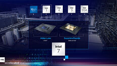
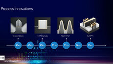
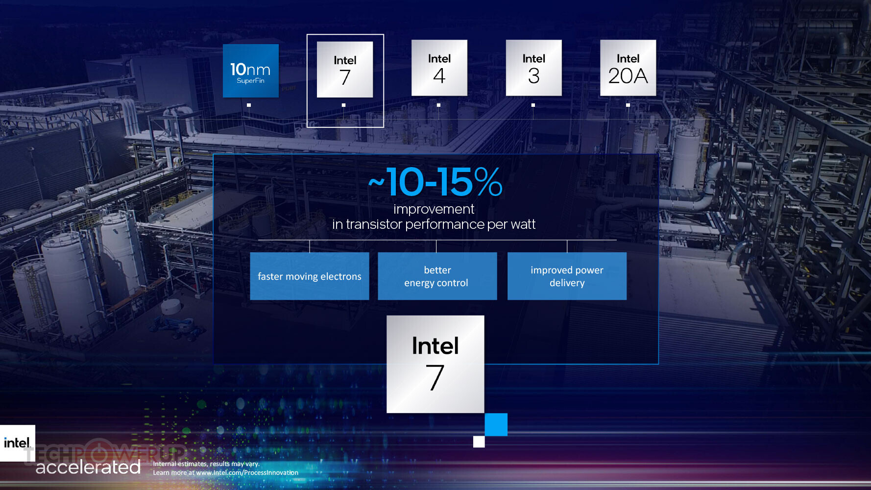
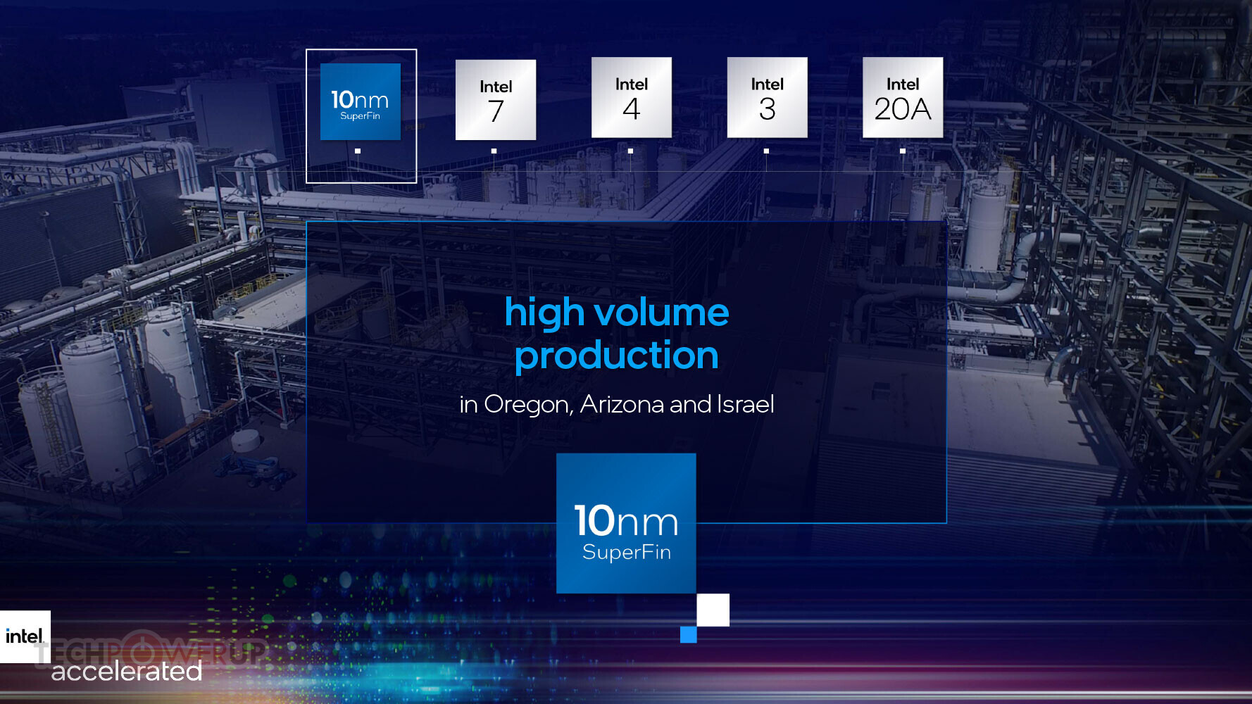
Intel's new foundry naming system sees its 10 nm Enhanced SuperFin node re-badge as "Intel 7." The company currently builds 11th Gen Core "Tiger Lake" processors on the 10 nm SuperFin node, and is expected to build its upcoming 12th Gen Core "Alder Lake" chips on its refinement, the 10 nm Enhanced SuperFin, which will now be referred to as "Intel 7." The company is careful to avoid using the nanometer unit next to the number, instead signaling the consumer that the node somehow offers transistor density and power characteristics comparable to a 7 nm node. Intel 7 offers a 10-15 percent performance/Watt gain over 10 nm SuperFin, and is already in volume production, with a debut within 2021 with "Alder Lake."
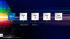
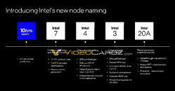

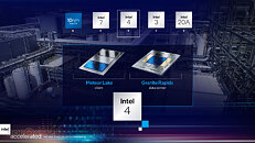

 This is where things get interesting. The successor to Intel 7 is named Intel 4, and is technically a 7 nm EUV node. This node offers a 20 percent performance/Watt gain over Intel 7 (aka 10 nm Enhanced SuperFin), and will debut in mid-2022 with "Meteor Lake" client- and "Granite Rapids" enterprise processors. Intel has gone with "4" for the name as 2022 sees both Samsung and TSMC roll out their sub-5 nm nodes. TSMC will debut the 4 nm, while Samsung will hopefully iron out its 5 nm yield issues, and ramp up 4 nm, by 2022.
 Intel 3 succeeds Intel 4 in the second half of 2023, and is timed to launch around the time TSMC comes out with its sub-4 nm node, likely the 2 nm. Intel claims this node offers an 18 percent performance/Watt gain over the Intel 4, implement a denser HP library, increase the use of EUV, improve the drive-current and via resistance, to result in the performance/Watt target. With no mention of FET size, it's very likely that Intel 3 is still a 7 nm node.


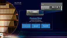
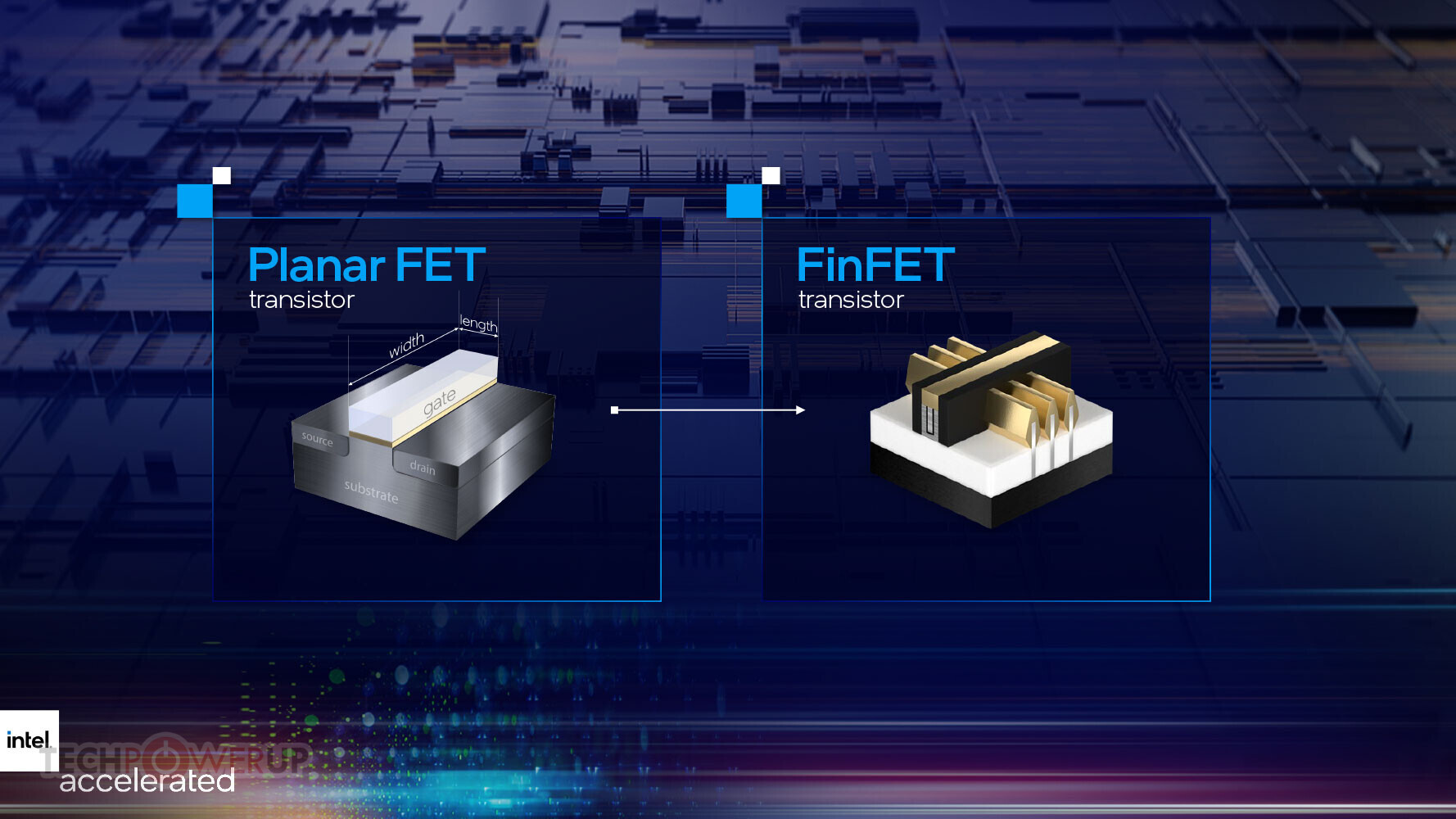
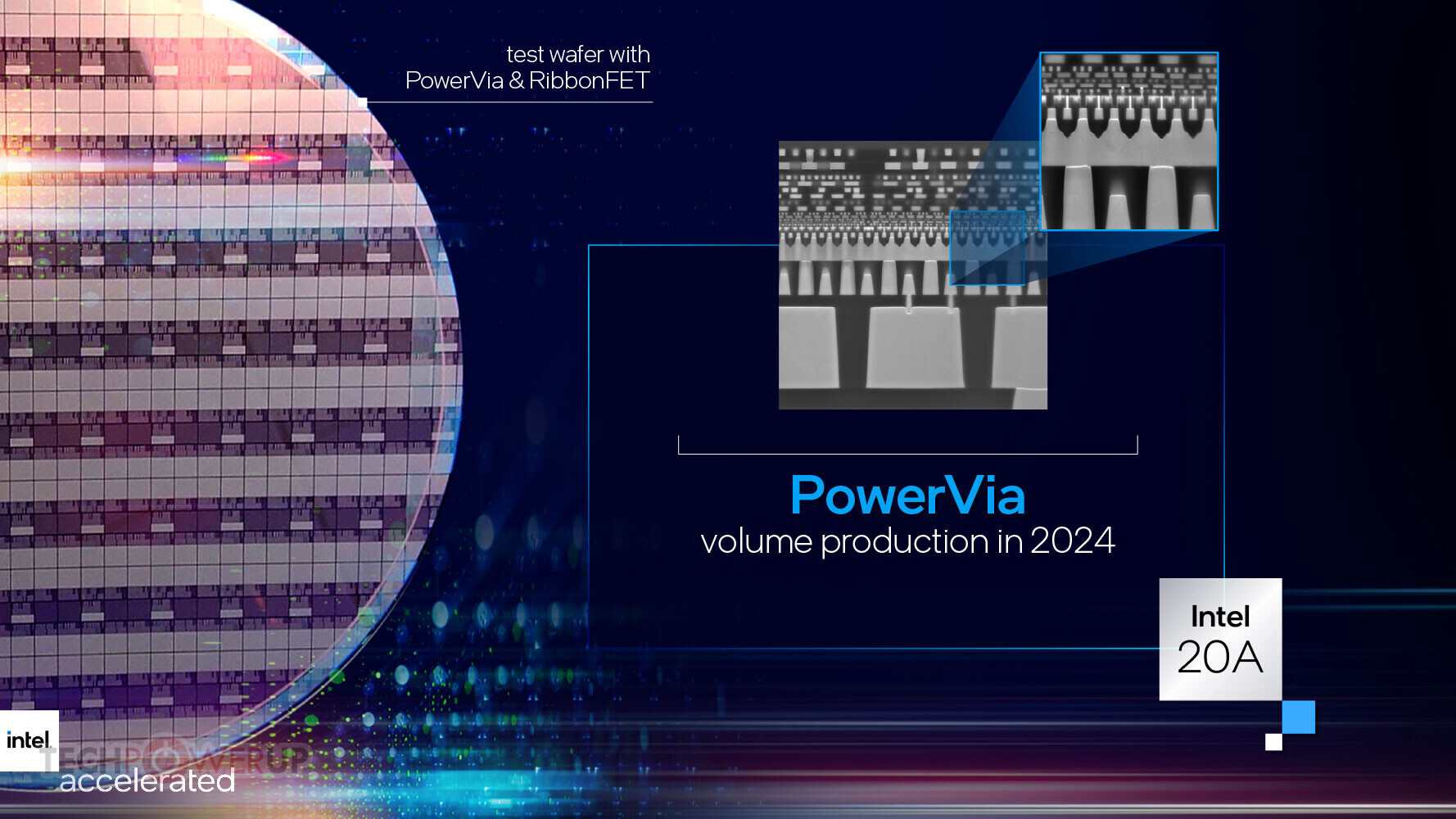
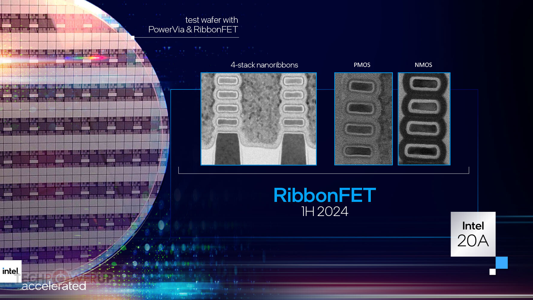
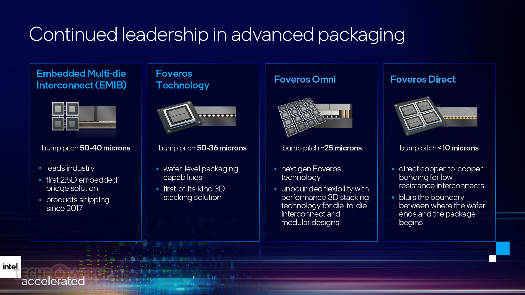
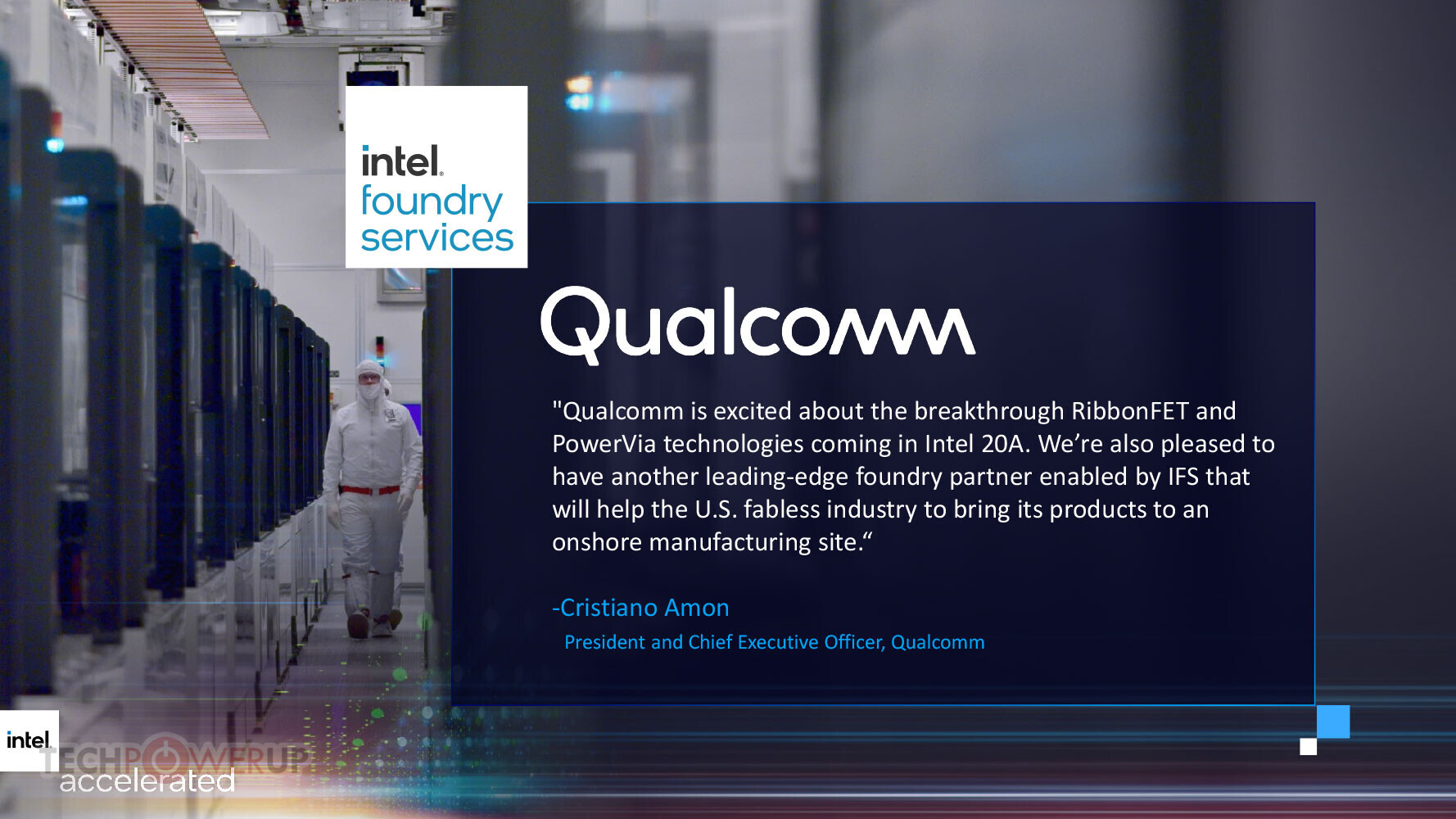
 It's only in 2024 that Intel is promising major technological breakthroughs, with Intel 20A, heralding the era in silicon fabrication where transistor sizes are measured in Angstroms (0.1 nm). 20A would hence be a creative way of saying 2 nm. Intel will introduce a brand new transistor design it calls the RibbonFET. It remains to be seen if this is a whole new innovation or similar to nanosheet FETs. Intel is also announcing PowerVia, a revolutionary new way to connect silicon dies with each other, or with the package, which debuts with the Intel 20A node. The company is targeting a 1H-2024 debut of this new node.
With these, Intel is ensuring that it has a new node to offer each year leading up to 2024, each with a double-digit percent performance/Watt gain, so the company can restore something resembling its "Tick-Tock" product development cadence, enabling it to compete not just against AMD, but also the emergence of serious Arm-powered rivals, such as NVIDIA, Qualcomm, and Apple. The company is hence facing similar levels of competition as the early 1990s. x86 may no longer have a stranglehold over the PC, as Arm-powered rivals claw away at market-share with efficient and fairly-powerful chips.
The complete slide-deck follows.


Source:
VideoCardz
Intel's new foundry naming system sees its 10 nm Enhanced SuperFin node re-badge as "Intel 7." The company currently builds 11th Gen Core "Tiger Lake" processors on the 10 nm SuperFin node, and is expected to build its upcoming 12th Gen Core "Alder Lake" chips on its refinement, the 10 nm Enhanced SuperFin, which will now be referred to as "Intel 7." The company is careful to avoid using the nanometer unit next to the number, instead signaling the consumer that the node somehow offers transistor density and power characteristics comparable to a 7 nm node. Intel 7 offers a 10-15 percent performance/Watt gain over 10 nm SuperFin, and is already in volume production, with a debut within 2021 with "Alder Lake."


With these, Intel is ensuring that it has a new node to offer each year leading up to 2024, each with a double-digit percent performance/Watt gain, so the company can restore something resembling its "Tick-Tock" product development cadence, enabling it to compete not just against AMD, but also the emergence of serious Arm-powered rivals, such as NVIDIA, Qualcomm, and Apple. The company is hence facing similar levels of competition as the early 1990s. x86 may no longer have a stranglehold over the PC, as Arm-powered rivals claw away at market-share with efficient and fairly-powerful chips.
The complete slide-deck follows.


101 Comments on Intel Rebadges 10nm Enhanced SuperFin Node as "Intel 7," Invents Other Creative Node Names
i do not care who will have the best product ... i care for the one who genuinely did something worth my time ... AMD did it two time (Athlon/Ryzen well three if counting the Athlon64 and Phenom which i quite liked but that one is more personal) Intel did it only once (first core gen) both had their huge fumbles (Bulldozer for the reds, Netburst for the blues )
How about real world applications. Apple M1, TSMC 5nm, 16 billion transistors, 119mm2 die, density = 135 million transistors per mm2.
AMD Ryzen CCD die, TSMC 7nm, 4.15 billion transistors, die size 80mm2, density = 51 million transistors/mm2.
Intel Ice Lake, Intel 10nm, transistor count estimated to be 7 billion (extrapolated from comments Jim Keller made about the transistor count of an Ice Lake core), die size 122mm2, density = 57 million transistors per mm2.
Subsequent Intel designs??? Who knows, because Intel stopped detailing the transistor count of its cores after Ice Lake, which I think is telling (they had no qualms doing so when they had the density lead over TSMC).
It shows that whilst Intel has previously indicated their OG 10nm process used on Cannonlake was 108million/mm2, the trend since then has been a reduction in density (in order to increase clocks) at the same time TSMC processes have continued to become denser. All indications are that Intel 10ESF is approx equal to TSMC 7nm, and definitely less dense than TSMC 5nm. That still places Intel a full node behind from a transistor density perspective.
I can't knock Intel for the naming scheme, after all Tsmc did the same.
However Tsmc can and likely will reply in marketing kind.
We're getting A20 off Tsmc in 2023.5 I'd wager, though it is not called that presently.
I think someone needs to legislate against this bullshit and inforce a density lead classification system.
They're not regulating they're own bullshit and consumers are having the wool pulled over their eyes with this nonsense so a government needs to step up.
Though let's be honest, Tiger Lake is actually the pretty good even if it consumes quite a bit more power.Nah, It makes more sense to just use 10nm ESF to get 'equivalent' to competitors.They are using GAA in 2nm which is scheduled for mid 2023. Samsung is the one that's going to try to get GAA first.
Plus everyone has been announcing it for sort of years.
See:www.anandtech.com/show/16823/intel-accelerated-offensive-process-roadmap-updates-to-10nm-7nm-4nm-3nm-20a-18a-packaging-foundry-emib-foveros/3
Another similar thing that irks me is with various signs about the 1m social distance. Here in Italy, half have distances (m, metres), half have either weights (”””””millitonnes””””””, mt XD) or magnetic flux density (megatesla, MT)
www.anandtech.com/show/15099/the-huawei-mate-30-pro-review-top-hardware-without-google/2
www.anandtech.com/show/7677/amd-kaveri-review-a8-7600-a10-7850k
Industry and technical analysts all are in a pretty nice agreement that Intel's 10nm is in the same group with TSMC/Samsung 7nm. Similarly Intel's 7nm in the same group with TSMC/Samsung 5nm.Mobile chips are from a different variation of manufacturing process. 90% of theoretical density is rather normal for that.
High performance chips come with a much lower density, from all manufacturers.
You are right about Intel not having real implementation with max density in a product . On the other hand, I have no idea what in their product portfolio would not be using the high performance variation. IIRC Intel has said their 10nm has two high performance variations with 80 MTr/mm2 and 65 MTr/mm2.
At the same time, I cannot think of anything from Samsung's 7nm that would be on high performance variation. The main use so far are the mobile SoCs. Can you think of something Samsung has manufactured?
Edit:
Apparently Intel did have a kind of product with high density in the 10nm failure times. i3-8121U had 100.8 MTr/mm2: Intel 10 nm Logic Process Analysis (Cannon Lake) | TechInsights
nm numbers are all marketing and Intel is pretending they're a performance indicator. This is an obvious attempt at obfuscation, b/c their nodes suck and has nothing to do with actual density (real or imagined).
10nm has such a bad reputation that it has to be relabeled.
They're yields could not even be marketed ffs where's Tsmc churned 7nm out a fair while productively and profitably before Intel ever got a worldwide 10nm release Soo better at what, in what way.
I'm ok with Intel tit for tatting Tsmc's naming scheme since what's good for the goose is indeed good for the gander but.
Fu#@ these companies, they're being dicks, use physics or a regulated naming convention s, not this mind f#£@ bull that's as clear and truthful as Abie Kruger or the value of bitcoin.
Alderlake chips look interesting on the big LITTLE core pairing I look forward to seeing how they benchmark some have more little cores, but fewer big cores and others are the opposite. Can the chip with more little cores and few big cores beat the one with more big cores and few little cores or does it vary largely based on workload? What's important here is the relative strength of a little core versus a big core in the design. Also how it impacts efficiency as well is important. Alderlake could end up the best of the best for DDR4 capable systems potentially especially on value so I'm keeping a careful eye on how they turn out.
Time will reveal how good or bad Alderlake is or what niche markets it might penetrate and be good consumer value or not. Intel might surprise a bit. The cache structure of the big and little cores could be interesting as well if they happen to be the same the chips with more little cores could be good in certain workloads due to that aspect more CPU cache in total helps a lot with NTFS compression speeds at certain I/O size and file sizes. I can be critical of Intel and they deserve their share of it, but they knock it out of the park sometimes. I'm not confident Alderlake will be that, but it could be another step back in the right direction at least and in the case of people wanting to continuing getting use out of their DDR4 hardware surprising value or cost savings.
The other aspect of big LITTLE for Intel is if they can better perfect this they can mix and match 10nm with a lower node and still once become a lot more competitive with AMD a lot more quickly. In the case of 10nm it's not perfect and has taken far longer than Intel would've preferred to reach even the maturity it is at now, but it still can improve. Perhaps they'll be able to do a few things to salvage it further was well through some discovery or break thru. It's not a lost cause, but prioritizing a lower node is important for them. Intel can't continue to hemorrhage voltage leakage due to being on such a more outdated node relative to competition.
Not everyone that buys from best buy is a noob, sometimes people don't have the time to build there own or don't want to support it themselves.
Alder Lake's smaller Gracemont cores jump forward a single Atom generation and offer the benefit of being more power and area efficient (perf/mm^2) than the larger Golden Cove cores. Gracemont also comes with increased vector performance, a nod to an obvious addition of some level of AVX support (likely AVX2). Intel also lists improved single-threaded performance for the Gracemont cores.