Tuesday, July 27th 2021

Intel Rebadges 10nm Enhanced SuperFin Node as "Intel 7," Invents Other Creative Node Names
Intel, in a move comparable to its competitors' Performance Rating system from the 1990s, has invented a new naming scheme for its in-house foundry nodes to claim technological parity with contemporaries such as TSMC and Samsung, that are well into the sub-10 nm class. Back in the i586 era, when Intel's competitors such as AMD and Cyrix, couldn't keep up with its clock-speeds yet found their chips to be somewhat competitive, they invented the PR (processor rating) system, with a logical number attempting to denote parity with an Intel processor's clock-speed. For example, a PR400 processor rating meant that the chip rivaled a Pentium II 400 MHz (which it mostly didn't). The last that the PR system made sense was with the final generation of single-core performance chips, Pentium 4 and Athlon XP, beyond which, the introduction of multi-core obfuscated the PR system. A Phenom X4 9600 processor didn't mean performance on par with a rival Intel chip running at an impossible 9.60 GHz.
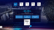
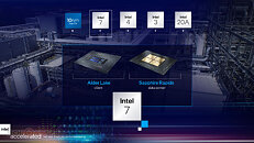
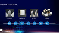
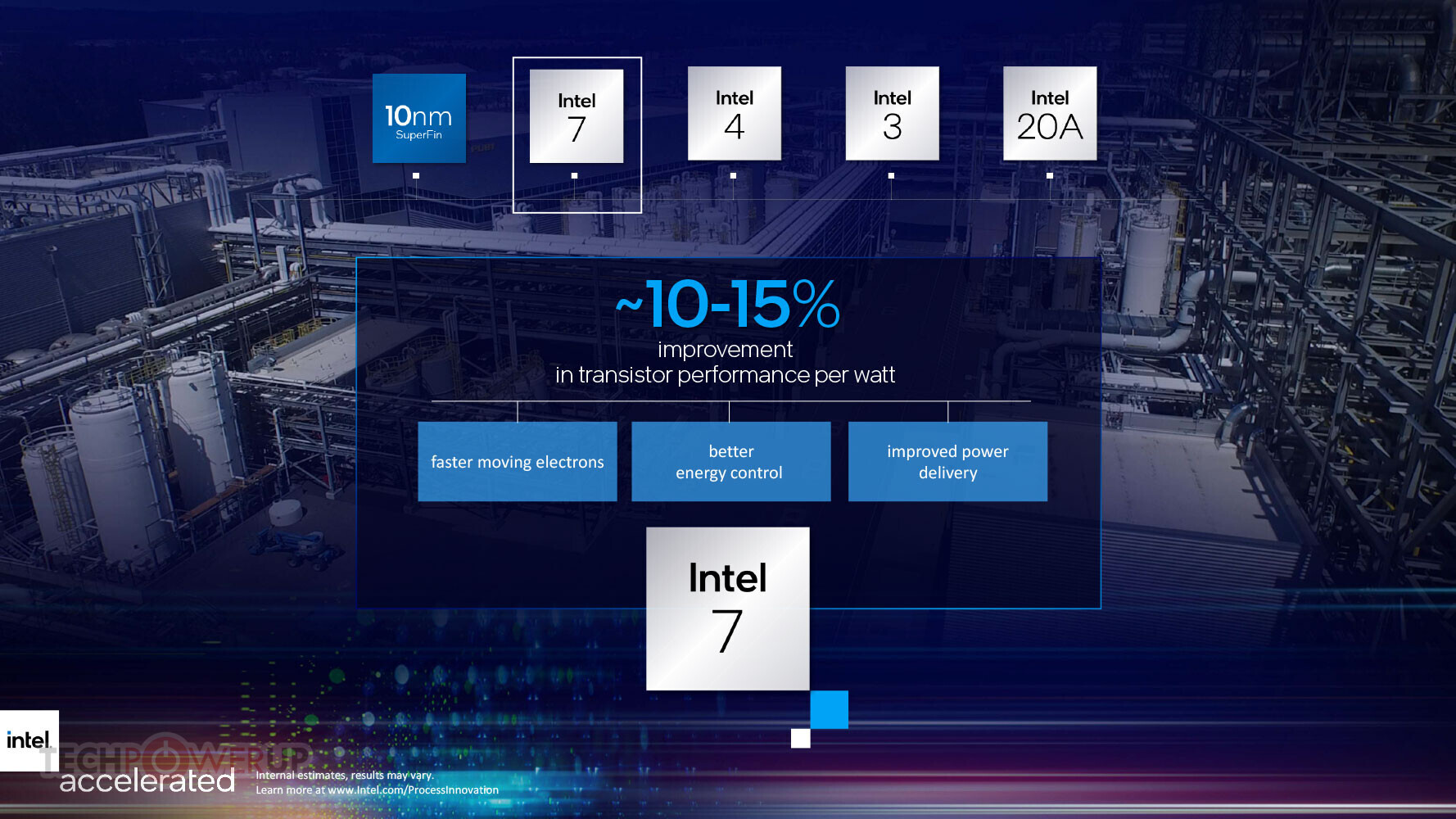
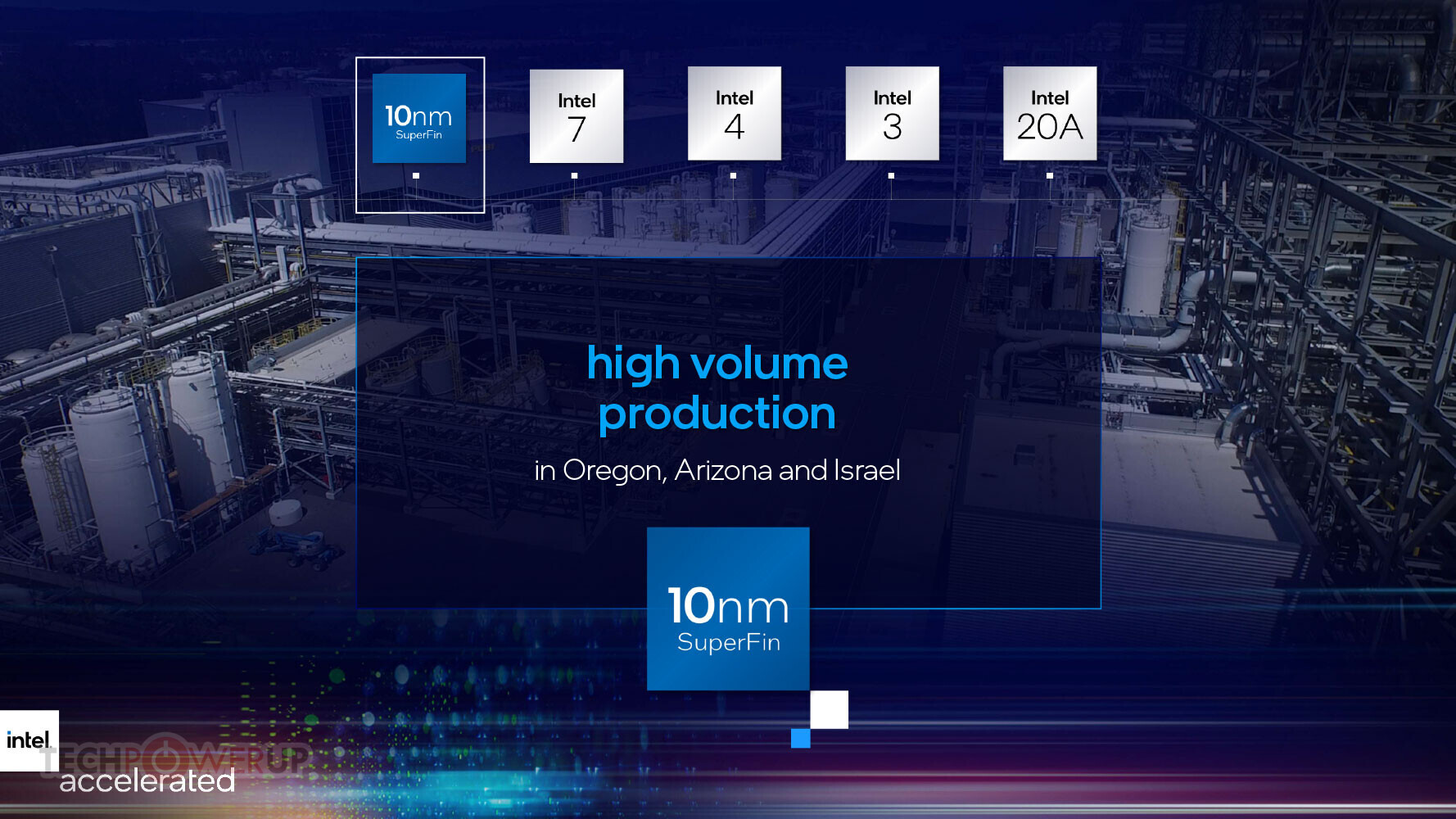
Intel's new foundry naming system sees its 10 nm Enhanced SuperFin node re-badge as "Intel 7." The company currently builds 11th Gen Core "Tiger Lake" processors on the 10 nm SuperFin node, and is expected to build its upcoming 12th Gen Core "Alder Lake" chips on its refinement, the 10 nm Enhanced SuperFin, which will now be referred to as "Intel 7." The company is careful to avoid using the nanometer unit next to the number, instead signaling the consumer that the node somehow offers transistor density and power characteristics comparable to a 7 nm node. Intel 7 offers a 10-15 percent performance/Watt gain over 10 nm SuperFin, and is already in volume production, with a debut within 2021 with "Alder Lake."
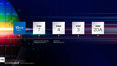
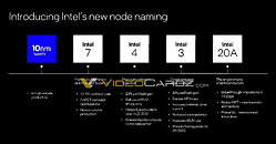
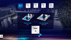

 This is where things get interesting. The successor to Intel 7 is named Intel 4, and is technically a 7 nm EUV node. This node offers a 20 percent performance/Watt gain over Intel 7 (aka 10 nm Enhanced SuperFin), and will debut in mid-2022 with "Meteor Lake" client- and "Granite Rapids" enterprise processors. Intel has gone with "4" for the name as 2022 sees both Samsung and TSMC roll out their sub-5 nm nodes. TSMC will debut the 4 nm, while Samsung will hopefully iron out its 5 nm yield issues, and ramp up 4 nm, by 2022.
 Intel 3 succeeds Intel 4 in the second half of 2023, and is timed to launch around the time TSMC comes out with its sub-4 nm node, likely the 2 nm. Intel claims this node offers an 18 percent performance/Watt gain over the Intel 4, implement a denser HP library, increase the use of EUV, improve the drive-current and via resistance, to result in the performance/Watt target. With no mention of FET size, it's very likely that Intel 3 is still a 7 nm node.

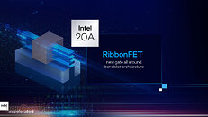
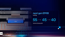
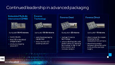
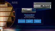
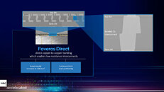
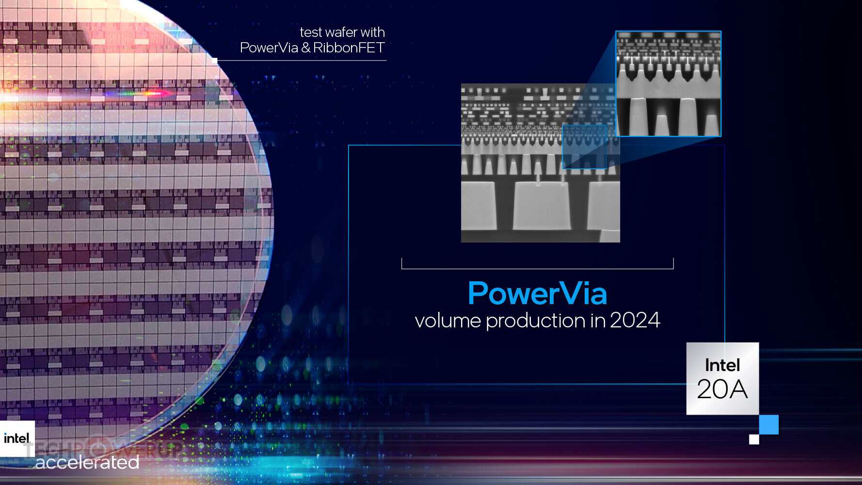
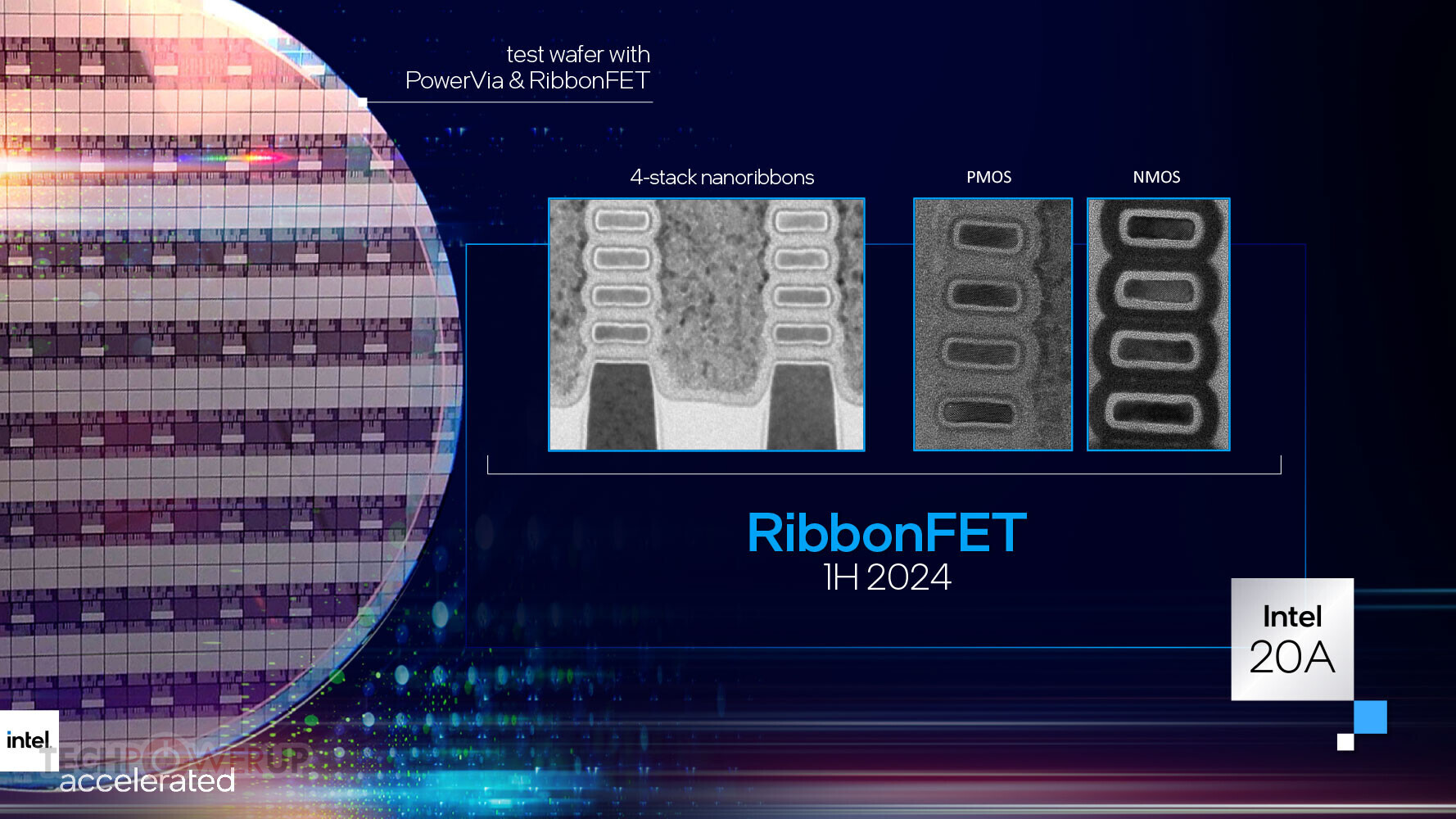
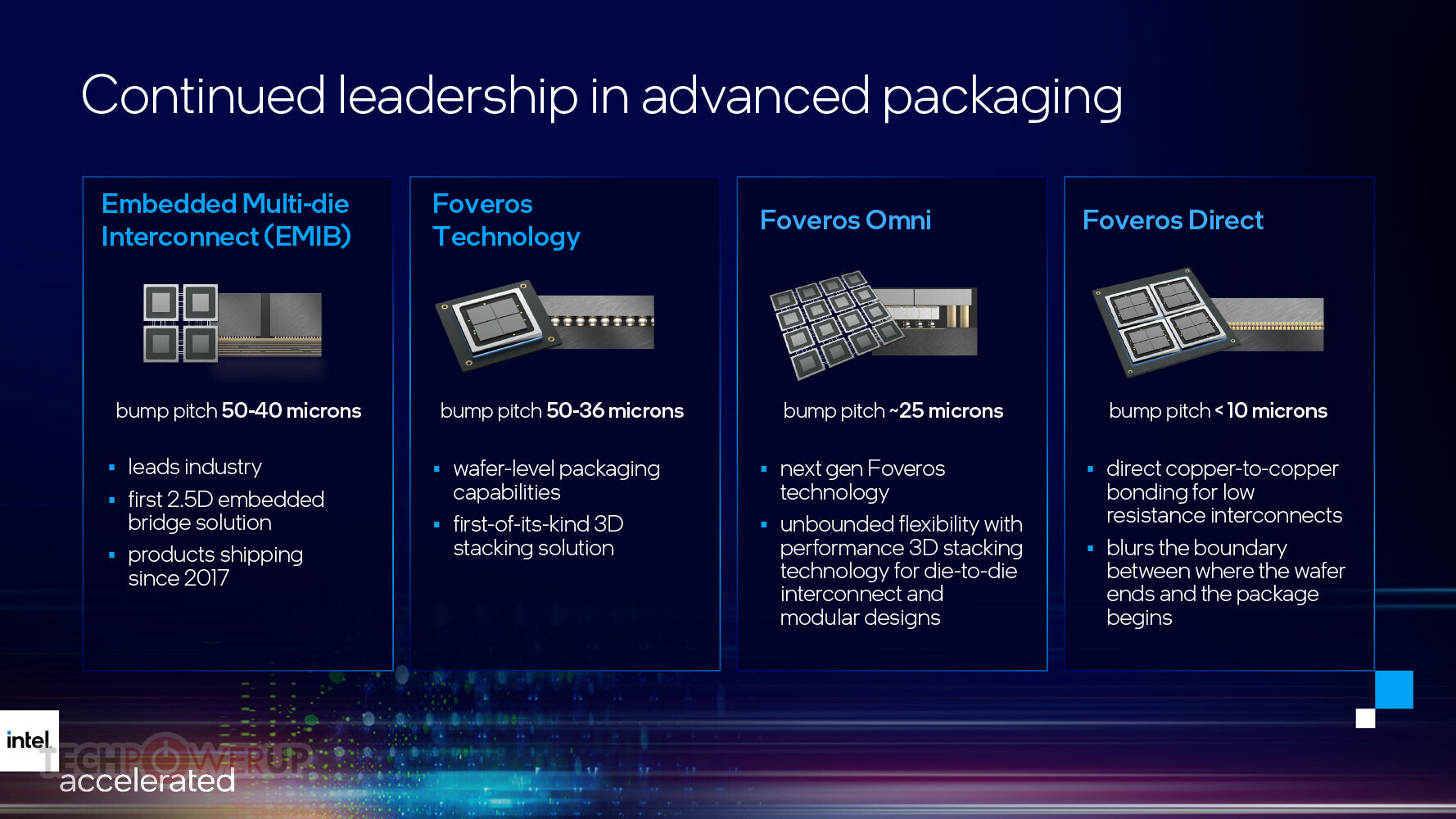
 It's only in 2024 that Intel is promising major technological breakthroughs, with Intel 20A, heralding the era in silicon fabrication where transistor sizes are measured in Angstroms (0.1 nm). 20A would hence be a creative way of saying 2 nm. Intel will introduce a brand new transistor design it calls the RibbonFET. It remains to be seen if this is a whole new innovation or similar to nanosheet FETs. Intel is also announcing PowerVia, a revolutionary new way to connect silicon dies with each other, or with the package, which debuts with the Intel 20A node. The company is targeting a 1H-2024 debut of this new node.
With these, Intel is ensuring that it has a new node to offer each year leading up to 2024, each with a double-digit percent performance/Watt gain, so the company can restore something resembling its "Tick-Tock" product development cadence, enabling it to compete not just against AMD, but also the emergence of serious Arm-powered rivals, such as NVIDIA, Qualcomm, and Apple. The company is hence facing similar levels of competition as the early 1990s. x86 may no longer have a stranglehold over the PC, as Arm-powered rivals claw away at market-share with efficient and fairly-powerful chips.
The complete slide-deck follows.


Source:
VideoCardz
Intel's new foundry naming system sees its 10 nm Enhanced SuperFin node re-badge as "Intel 7." The company currently builds 11th Gen Core "Tiger Lake" processors on the 10 nm SuperFin node, and is expected to build its upcoming 12th Gen Core "Alder Lake" chips on its refinement, the 10 nm Enhanced SuperFin, which will now be referred to as "Intel 7." The company is careful to avoid using the nanometer unit next to the number, instead signaling the consumer that the node somehow offers transistor density and power characteristics comparable to a 7 nm node. Intel 7 offers a 10-15 percent performance/Watt gain over 10 nm SuperFin, and is already in volume production, with a debut within 2021 with "Alder Lake."


With these, Intel is ensuring that it has a new node to offer each year leading up to 2024, each with a double-digit percent performance/Watt gain, so the company can restore something resembling its "Tick-Tock" product development cadence, enabling it to compete not just against AMD, but also the emergence of serious Arm-powered rivals, such as NVIDIA, Qualcomm, and Apple. The company is hence facing similar levels of competition as the early 1990s. x86 may no longer have a stranglehold over the PC, as Arm-powered rivals claw away at market-share with efficient and fairly-powerful chips.
The complete slide-deck follows.


101 Comments on Intel Rebadges 10nm Enhanced SuperFin Node as "Intel 7," Invents Other Creative Node Names
Transistor density of the node is not everything, architecture has a great impact. (e.g. AMD used to cram lots more transistors in Polaris than NV did with Pascal)
That is why L1 cache vs L1 cache was compared.
And, it was 22 by 22 for "7nm TSMC" and 24 by 24 for "14nm Intel". (yes, FOURTEEN, not ten)
Intel's 10nm might be closer to actual 7nm, than TSMC's.
10 = 7 when truth isn't a requirement :)
That is back to the point i made. Only the real world performance (and power consumption) matter, not the number on the fabrication node.
I thought Intel hired an Engineer to take the helm, not a marketing guy.
Don't try to drive your message home too hard. Power is indeed the best benchmark to size good foundries.
We can let the performance speak for itself in marketing. It will right itself anyway in regard to the goals it delivered upon.
Now let’s start being less transparent with our customers.
Great ideas coming out of Intel.
The wool hasn’t been pulled over your eyes yet?
I didn’t realize we are fighting tooth and nail about anything…
My stance is I want customer transparency and node plays in to power consumption. Your stance is, no no no there is more!!! Obviously. I never argued there wasn’t. Where was I fighting tooth and nail?
What is going to be different is the information gap between foundry node scaling factor and marketing factor will close because let us accept that it was always a marketing tool in the first place. Now, Intel won't market what it cannot deliver, so we will stop focusing whether the new node is 2.7 times, or 2.4 times more advanced in regard to the former one. This was a substitution for the real factor which was the cell size, not the Moore's Law like you accept it. It never was constant, it was just how Intel demonstrated it to be since they never, actually, wanted to be good, only "good enough", when in comparison to IBM when this numeric codes first sprung up.This is what Intel wants you to believe it to be since IBM times is all I'm saying. There is nothing transparent about it is all I'm saying. It is just a marketing 'hook'..
Samsung's 7nm may not have high power chip, but their 8nm has 350W+ chip with 46MT/mm2 [Nvidia A102 Chip]. What is the density of Intel's 28W-45W Tiger Lake chips??? And TSMC's 7nm has chip with 400W+ with 60MT/mm2+ [Nvidia A100 Chip, AMD Renoir, Cezenne] and and 80MT/mm2+ mobile SoC's[Huawei Kirin 990 5G,980 kwown]. What is on Intel's 10nm Lake field?? It was low power mobile chip and according to this photo [not official, take a grain of salt] it has only 49.39 MT/mm2 same or lower then TSMC's 10nm. Nowhere near as TSMC's 7nm.
According to same kind of analyst cold fusion is also possible[But only on paper, no real implementation and not possible according to physics].Just repeating Intel's marketing slide. No real analysis.
Intel 7. So its an i7 on Intel 7. You can really tell and see Pat's engineering influence is working out just fine. So glad they have real brains up there now. Even my 8700K feels a bit faster being on Intel 14 now. Fat Fins instead of Super, but still. Thanks, Pat!And yet it doesn't perform as such, strange how that works then. It underlines that architecture indeed has impact. The choice of what you place on a die, for example, also determines the density. Regardless, TSMC is producing 7nm on an EUV process and ever since DUV was left behind, the node performs as it should compared to its predecessors.
So forget density, start thinking lithography and how to get there. Its the chip quality that determines the frequency options for example, and the binning.