Saturday, March 8th 2025

China Develops Domestic EUV Tool, ASML Monopoly in Trouble
China's domestic extreme ultraviolet (EUV) lithography development is far from a distant dream. The newest system, now undergoing testing at Huawei's Dongguan facility, leverages laser-induced discharge plasma (LDP) technology, representing a potentially disruptive approach to EUV light generation. The system is scheduled for trial production in Q3 2025, with mass manufacturing targeted for 2026, potentially positioning China to break ASML's technical monopoly in advanced lithography. The LDP approach employed in the Chinese system generates 13.5 nm EUV radiation by vaporizing tin between electrodes and converting it to plasma via high-voltage discharge, where electron-ion collisions produce the required wavelength. This methodology offers several technical advantages over ASML's laser-produced plasma (LPP) technique, including simplified architecture, reduced footprint, improved energy efficiency, and potentially lower production costs.
The LPP method relies on high-energy lasers and complex FPGA-based real-time control electronics to achieve the same result. While ASML has refined its LPP-based systems over decades, the inherent efficiency advantages of the LDP approach could accelerate China's catch-up timeline in this critical semiconductor manufacturing technology. When the US imposed sanctions on EUV shipments to Chinese companies, the Chinese semiconductor development was basically limited as standard deep ultraviolet (DUV) wave lithography systems utilize 248 nm (KrF) and 193 nm (ArF) wavelengths for semiconductor patterning, with 193 nm immersion technology representing the most advanced pre-EUV production technique. These longer wavelengths contrast with EUV's 13.5 nm radiation, requiring multiple patterning techniques to achieve advanced nodes.
 However, this Huawei system must still answer questions about resolution capabilities, throughput stability, and integration with existing semiconductor manufacturing flows. However, commercializing an alternative EUV lithography tool will challenge ASML's position. ASML's latest High-NA EUV tool costs around 380 million US Dollars. No matter the cost for Chinese R&D centers, the Huawei EUV machine will deliver the much-needed upgrade path for the older DUV scanners, which previously limited domestic chip production. Despite China's development of solid IP, its manufacturing progress was limited, but it could experience a "DeepSeek" moment very soon. Leading fabs like SMIC are working with Huawei to integrate the EUV scanners into existing workflows. A solid semiconductor manufacturing workflow takes years to build, so we have to see what the final result will be.
Source:
Yin Sun
The LPP method relies on high-energy lasers and complex FPGA-based real-time control electronics to achieve the same result. While ASML has refined its LPP-based systems over decades, the inherent efficiency advantages of the LDP approach could accelerate China's catch-up timeline in this critical semiconductor manufacturing technology. When the US imposed sanctions on EUV shipments to Chinese companies, the Chinese semiconductor development was basically limited as standard deep ultraviolet (DUV) wave lithography systems utilize 248 nm (KrF) and 193 nm (ArF) wavelengths for semiconductor patterning, with 193 nm immersion technology representing the most advanced pre-EUV production technique. These longer wavelengths contrast with EUV's 13.5 nm radiation, requiring multiple patterning techniques to achieve advanced nodes.

58 Comments on China Develops Domestic EUV Tool, ASML Monopoly in Trouble
The hacker news bite deep. :roll:
It makes your previous arguments irrelevent.
Because official CCP sources also receive orders to publish propaganda.
Below is a picture of the CCP official (Vice Minister of Foreign Affairs of China) claiming they did not steal, did not rob, did not lie on their achievements.
So
If 'official sources also receive orders to publish propaganda' is true, then........THEY DID, and your previous arguments are irrelevent.
and,
If 'official sources also receive orders to publish propaganda' isn't true, then you just lied.
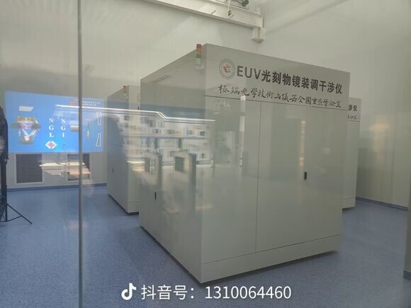
From the picture in the OP, that translates to EUV lithography objective lens mounting interferometer.
It is one part of a machine of an assembly line of manufacturing the lens for EUV lithography.
It is NOT an EUV tool at all.
It is a tool to make one of the tools that goes into the actual EUV tool.
And ASML don't even make interferometer.
Companies like Canon and Ushio made these and supply to various tool manufacturers.
It is like claiming you are able to manufacture a whole car but the only thing you showed us is a machine for making brake handles.
Yes it is an part of the car, but No that's not the whole car and it doesn't make you a car manufacturer.