Saturday, March 8th 2025

China Develops Domestic EUV Tool, ASML Monopoly in Trouble
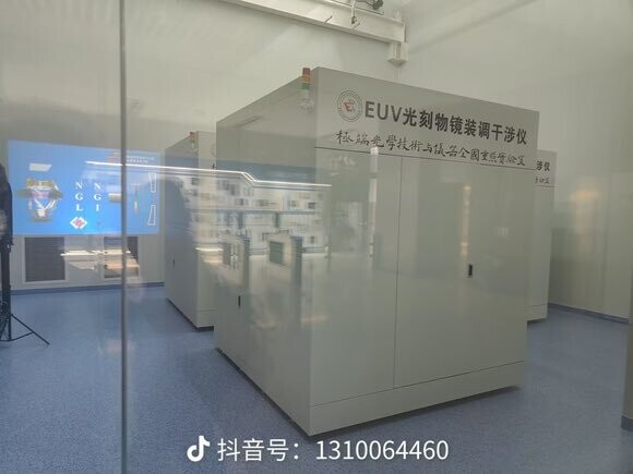
China's domestic extreme ultraviolet (EUV) lithography development is far from a distant dream. The newest system, now undergoing testing at Huawei's Dongguan facility, leverages laser-induced discharge plasma (LDP) technology, representing a potentially disruptive approach to EUV light generation. The system is scheduled for trial production in Q3 2025, with mass manufacturing targeted for 2026, potentially positioning China to break ASML's technical monopoly in advanced lithography. The LDP approach employed in the Chinese system generates 13.5 nm EUV radiation by vaporizing tin between electrodes and converting it to plasma via high-voltage discharge, where electron-ion collisions produce the required wavelength. This methodology offers several technical advantages over ASML's laser-produced plasma (LPP) technique, including simplified architecture, reduced footprint, improved energy efficiency, and potentially lower production costs.
The LPP method relies on high-energy lasers and complex FPGA-based real-time control electronics to achieve the same result. While ASML has refined its LPP-based systems over decades, the inherent efficiency advantages of the LDP approach could accelerate China's catch-up timeline in this critical semiconductor manufacturing technology. When the US imposed sanctions on EUV shipments to Chinese companies, the Chinese semiconductor development was basically limited as standard deep ultraviolet (DUV) wave lithography systems utilize 248 nm (KrF) and 193 nm (ArF) wavelengths for semiconductor patterning, with 193 nm immersion technology representing the most advanced pre-EUV production technique. These longer wavelengths contrast with EUV's 13.5 nm radiation, requiring multiple patterning techniques to achieve advanced nodes.
 However, this Huawei system must still answer questions about resolution capabilities, throughput stability, and integration with existing semiconductor manufacturing flows. However, commercializing an alternative EUV lithography tool will challenge ASML's position. ASML's latest High-NA EUV tool costs around 380 million US Dollars. No matter the cost for Chinese R&D centers, the Huawei EUV machine will deliver the much-needed upgrade path for the older DUV scanners, which previously limited domestic chip production. Despite China's development of solid IP, its manufacturing progress was limited, but it could experience a "DeepSeek" moment very soon. Leading fabs like SMIC are working with Huawei to integrate the EUV scanners into existing workflows. A solid semiconductor manufacturing workflow takes years to build, so we have to see what the final result will be.
Source:
Yin Sun
The LPP method relies on high-energy lasers and complex FPGA-based real-time control electronics to achieve the same result. While ASML has refined its LPP-based systems over decades, the inherent efficiency advantages of the LDP approach could accelerate China's catch-up timeline in this critical semiconductor manufacturing technology. When the US imposed sanctions on EUV shipments to Chinese companies, the Chinese semiconductor development was basically limited as standard deep ultraviolet (DUV) wave lithography systems utilize 248 nm (KrF) and 193 nm (ArF) wavelengths for semiconductor patterning, with 193 nm immersion technology representing the most advanced pre-EUV production technique. These longer wavelengths contrast with EUV's 13.5 nm radiation, requiring multiple patterning techniques to achieve advanced nodes.

90 Comments on China Develops Domestic EUV Tool, ASML Monopoly in Trouble
China leads the world In 37 out of 44 critical
technologies
China leads the world in 37 out of 44 critical TechnologiesChina's advantage is their government has "5 year" plans. (They are on#15 now).
in 2015, Beijing’s launched its "Made in China 2025" strategic plan aimed to transform the country from a low-cost manufacturing base into a high-tech superpower. Ten key focus industries have been identified, spanning
advanced computing,
aerospace,
artificial intelligence and
green energy (including electric vehicles).
Since then, Chinese companies – the likes of BYD, Tencent and Huawei – have become dominant global players in these arenas
In a democracy where the government changes every 4 to 8 years it's impossible to set long-term goals
For example Biden used government subsidies to encourage Americans to turn to electric vehicles. Now Trump is undoing everything to Biden tried to do
ASML Laser-Produced Plasma (LPP) Method
This method is like using a powerful flashlight to shine on a mirror ball coated with tiny droplets. The flashlight (a high-energy laser) hits the droplets (liquid tin), turning them into a glowing mist (plasma). This glowing mist scatters light (EUV) all over the room. However, the flashlight needs to be incredibly powerful, and the process involves a lot of intricate machinery, like advanced circuits (FPGA chips), to ensure everything happens precisely. This makes it highly effective but also very complex and expensive.
China's Laser-Induced Discharge Plasma (LDP) Method
Now imagine instead of a flashlight, you use a simple spark between two wires
First, a small vapor cloud (tin) is released between the wires.
Then, a spark (high voltage) is applied, turning the vapor into a glowing cloud (plasma) that lights up the room (produces EUV light).
This method directly converts electricity into light, making it simpler and more energy-efficient.
However, it’s like trying to adjust the timing of the spark and the amount of vapor perfectly—it’s tricky to get just right. Additionally, some worry that this spark-based method might not be bright enough to light up a very large room (power output limitations).
Comparison
LPP (Flashlight on droplets): Complex, powerful, and precise but expensive and energy-intensive.
LDP (Spark in a vapor cloud): Simpler, cheaper, and more energy-efficient but technically challenging to optimize and potentially limited in brightness.
whoosh if I ever saw one
where do you think the tech came from
www.latimes.com/business/autos/la-fi-hy-elon-musk-opens-tesla-patents-20140612-story.html
:rolleyes:
indico-cdex.ep.tsinghua.edu.cn/event/38/contributions/214/attachments/144/206/Tang-SSMBActivitiesatTsinghuaUniversity.pdf
China is aiming to leap-frog current top-end EUV technologies with steady-state microbunching (SSMB) EUV, that would give China what's been called a "lithographic cannon", enabling faster, higher-yield, and cheaper production of cutting-edge 2nm-and-lower microchips.
But I highly doubt the truthfulness of this piece when the person making this pdf can't even keep the word 'Content' in a single line.
Still skeptical?
After seeing China's progress from living in a swamp to lead almost every single industry in the world (except semiconductors) in 20-30 years, we thought a few trade restrictions would stop them from taking the lead in semiconductors?
We just made the bear angry. And the told them we want to humiliate them for another 100+ years.
I read this quote that there has never been the rise of any empire like this without a war, instead they achieved it with sheer tenacity and hard work. We can't believe they wouldn't want to impose themselves on the world and turn other nations into slaves or take advantage of them, because that's what we would do if we were in their position.
OK great, so we made an enemy out of them. So what, we're going to keep trolling them and hope they are never able to dominate the last industry they want? To help ourselves sleep at night? How dumb and arrogant can we be.
So, ok you ban your tech to China , so that you maintain leadership. Ok fine , excellent!
But , what do you do yourself ,once you slowed down your opponent? Do you make efforts
to increase your own speed? I don't think so . If the "West" was really concerned about its
silicon manufacturing prowess, it would try to make EUV machines in the US , in the UK , in Germany
and so on .
But they don't . They rely on the island of Taiwan, at least superficially . How stupid is that?
The claim that making EUV machines is still 10 years away for China is laughable on so many levels
it is already sad.
1st the scientific and industrial base of China is more than enough to make it in 10 years or earlier. But let's
suppose it happens after 15 years( I really doubt it will be delayed by that much but anyway). If you are not going to be
in a better position after 15 years , this means that all your efforts were in vain . Especially if you are still reliant on the Netherlands
and Taiwan.
2nd I am pretty certain , that all of the above is understood, exactly like this at the higher echelons, that take the decisions.
So, this means they know and they don't care. Maybe they don't care, because they know sth we don't know.
And this is certainly not the "it is very difficult to build EUV lithography". I mean, come on how difficult can it be ?
You are not asking it from the semi-savage tribes of the Amazon , this is China my friends.
It is as effcient and buys equivalent intellectual power.